
Shift register, shift register array, and flat display apparatus

Active Publication Date: 2008-03-20
AU OPTRONICS CORP
View PDF2 Cites 32 Cited by
  • Summary
  • Abstract
  • Description
  • Claims
  • Application Information

AI Technical Summary

Benefits of technology

[0012]According to the aforementioned configuration, this invention can reduce the coupling effect generated by the clock signal at the output terminal of the shift register. In addition, the falling time of the output waveform is shortened.

Problems solved by technology

However, due to the high cost of these drivers, alternative devices are proposed.
When applying the integrated driving circuit to a large sized liquid crystal display apparatus, a large amount of power is required.
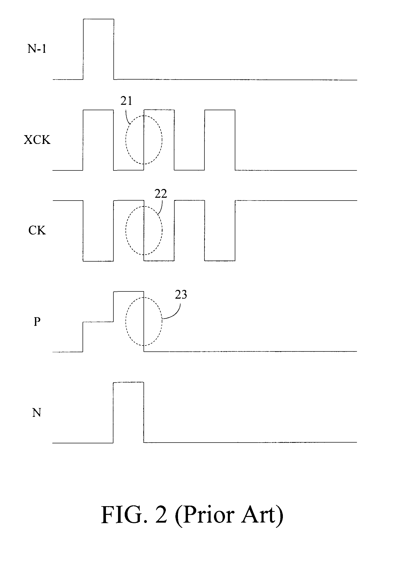
Unfortunately, by using this approach, the output waveform of the shift register generates a coupling effect which causes the LCD to function abnormally.
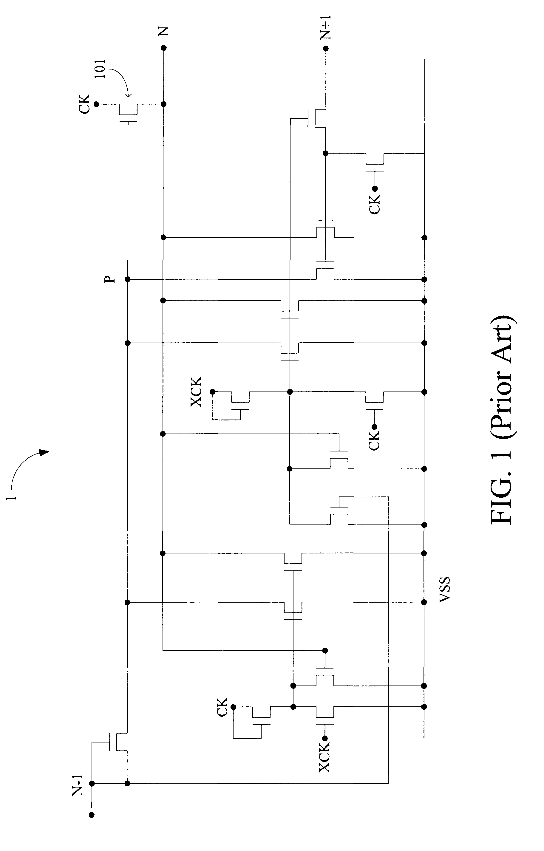
When the shift register 1 is applied to a large sized LCD, this design faces two serious defects.
The falling time is too long for a LCD.
Furthermore, when the size of the transistor 101 is enlarged, the coupling effect of the output terminal N becomes more significant, further causing erroneous operation of the next shift register, which considerably affects display quality.
According to the aforementioned problems and descriptions, the coupling effect and the long falling time of the output waveform are two common defects of current shift registers in LCDs.

Method used


Image

  • Shift register, shift register array, and flat display apparatus
  • Shift register, shift register array, and flat display apparatus
  • Shift register, shift register array, and flat display apparatus

Examples


Embodiment Construction

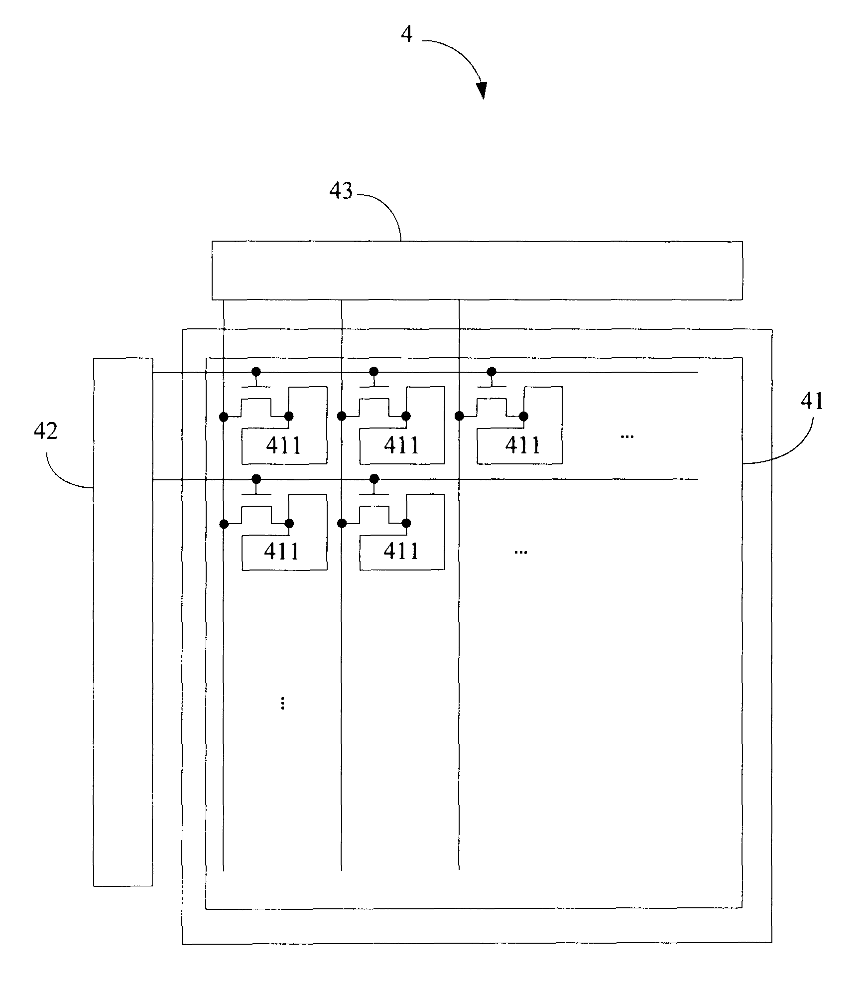
[0023]A first embodiment of this invention is a flat display apparatus, such as an LCD. The LCD comprises a display panel 4 as shown in FIG. 4A. The display panel 4 comprises a display array 41, a gate driving circuit 42 and a data driving circuit 43. The display array 41 comprises a plurality of pixels 411. FIG. 4B shows a shift register array 44 comprised in the gate driving circuit 42. The shift register array 44 comprises a plurality of shift registers 45. Each output of these shift registers 45 is coupled to an input of next shift register 45 except the last stage shift register 45. A connection relationship in these shift registers 45 is well known to those skilled in the art and thus is not detailed here. Each of these shift registers 45 is used to drive one row of pixels of the display array. For example, an N-th shift register 45 is used to drive an N-th row of pixels.

[0024]In general, a structure for each of the shift registers 45 is the same, but not limited to. However, ...


PUM


Abstract

A flat display apparatus comprising a shift register array is provided. The shift register array comprises a plurality of shift registers. At least one of these shift registers comprises a shift register unit, a first TFT, and a second TFT. The shift register unit is configured to receive an activation signal and comprises a first output terminal and a second output terminal. The gate of the first TFT is coupled to the first output terminal. The second electrode of the first TFT receives a clock signal. The gate of the second TFT is coupled to the first electrode of the first TFT. The second electrode of the second TFT is coupled to the second electrode of the first TFT. The first electrode of the second TFT is coupled to the second output terminal.

Description

CROSS REFERENCE TO RELATED APPLICATION[0001]This application claims priority to Taiwan Patent Application No. 095134023 filed on 14 Sep. 2006, the disclosure of which is incorporated herein by reference in its entirety.BACKGROUND OF THE INVENTION[0002]1. Field of the Invention[0003]The present invention relates to a flat display apparatus, specifically to a shift register of a shift register array.[0004]2. Descriptions of The Related Art[0005]Currently, most Liquid Crystal Displays (LCD) are equipped with a gate driver and a source driver to generate a gate pulse signal and a data signal. However, due to the high cost of these drivers, alternative devices are proposed. For example, a shift register fabricated on a glass substrate with circuit functions equivalent to a gate driver, called integrated driving circuit, is one of the alternatives.[0006]When applying the integrated driving circuit to a large sized liquid crystal display apparatus, a large amount of power is required. Cons...

Claims


Application Information

Patent Timeline
IPC IPC(8): G09G3/36
CPCG09G3/3677G11C19/28G09G2310/0286
Inventor CHEN, JING RUCHANG, LEE HSUNCHEN, SHYH-FENGCHANG, CHUN-JONGCHENG, YUNG-TSE
Owner AU OPTRONICS CORP
Learn More