
Rigid wave pattern design on chip carrier substrate and printed circuit board for semiconductor and electronic sub-system packaging

a technology of printed circuit board and chip carrier substrate, which is applied in the direction of solid-state devices, basic electric elements, electrical apparatus construction details, etc., can solve the problems of package having to be discarded, small form factor packages require very thin dice, and deformation of stress within dice, so as to reduce the deformation and stress, and the effect of reducing the cracking of the di

Active Publication Date: 2008-03-06
SANDISK TECH LLC
View PDF17 Cites 5 Cited by
  • Summary
  • Abstract
  • Description
  • Claims
  • Application Information

AI Technical Summary

Benefits of technology

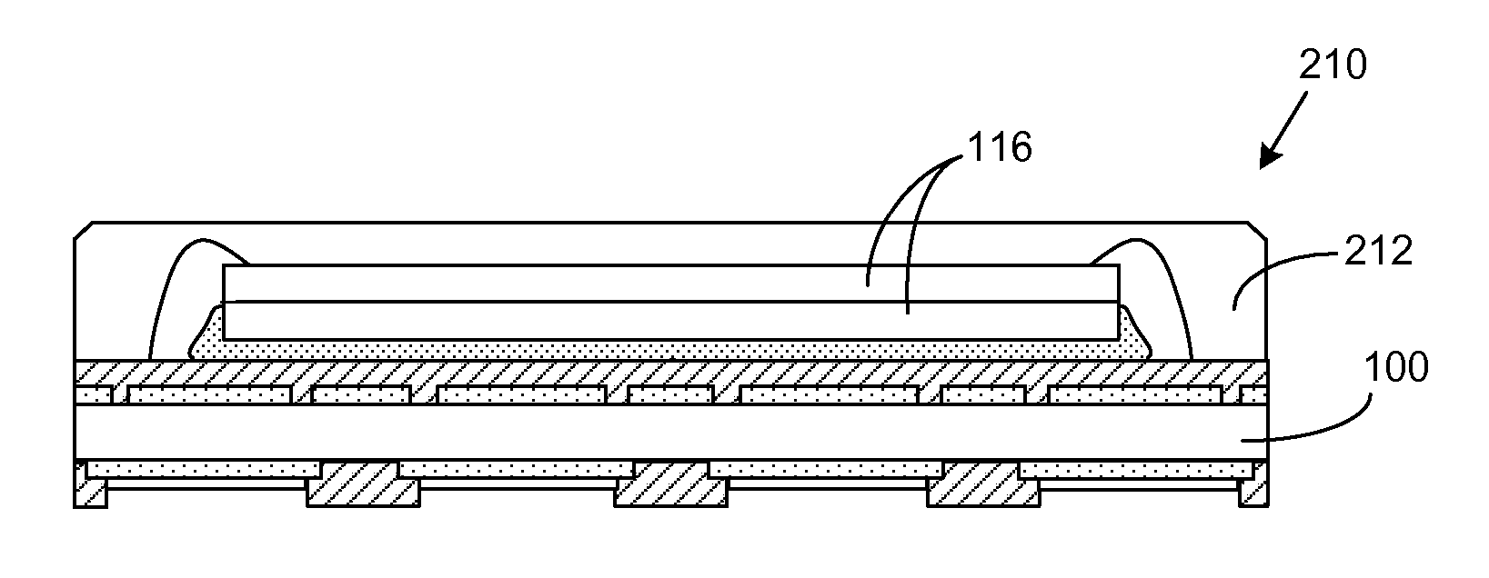
The invention is a strengthened semiconductor die package that includes a substrate with conductive layers and a rigid wave pattern to reduce deformation and stress on the die during the molding process. The rigid wave pattern is formed in a first surface of the substrate to align with and overlie the contact fingers formed on the opposite surface of the substrate. The etched portions of the rigid wave pattern have a distinct shape that helps alleviate die cracking. The advantages of this invention include reduced die cracking, improved reliability, and improved performance without any additional processing steps or fabrication costs.

Problems solved by technology

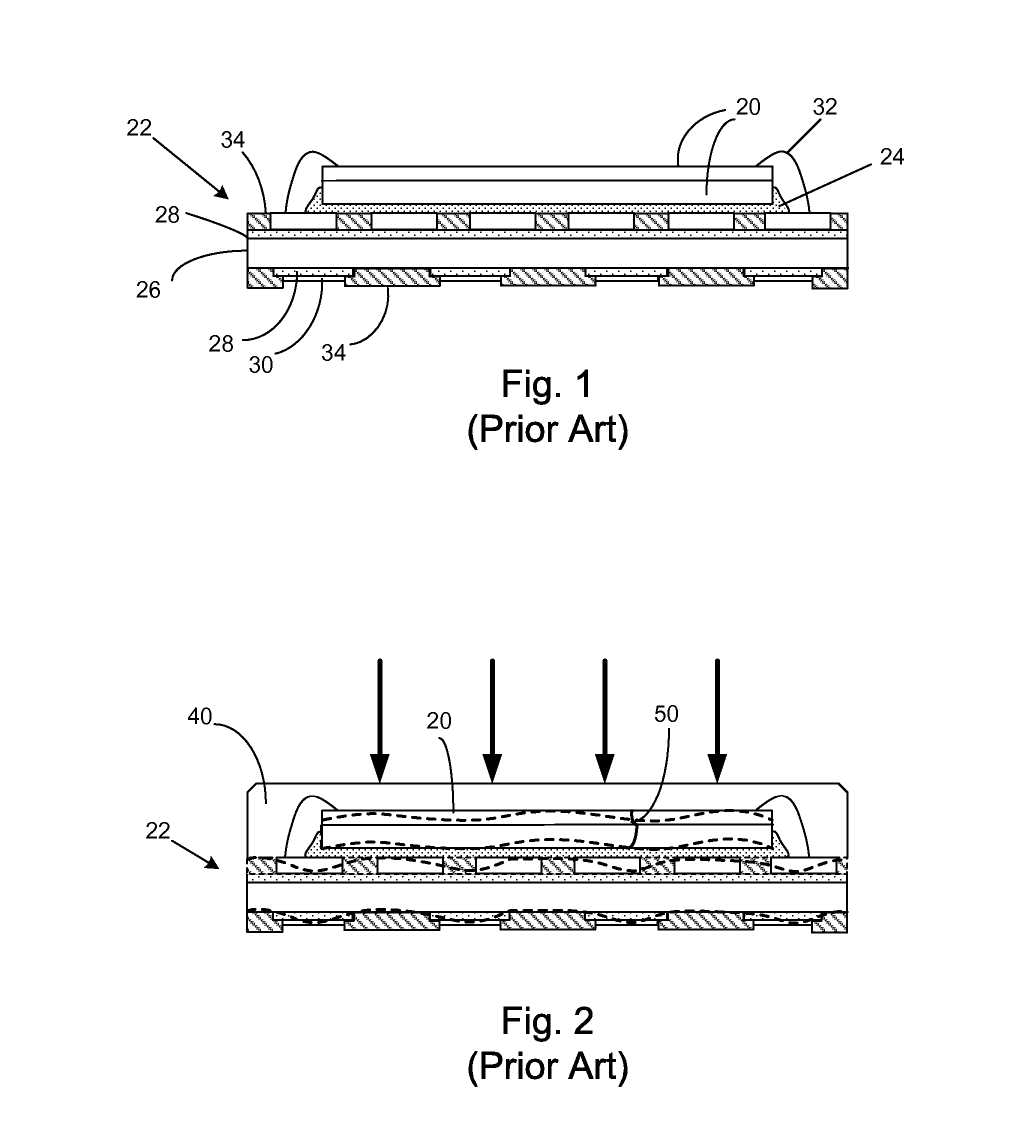
This results in stress buildup within the dice at positions in the dice located over the contact fingers.
However, chip scale packages (CSP) and the constant drive toward smaller form factor packages require very thin dice.
Die cracking under the stress of the molding process will generally result in the package having to be discarded.
Occurring at the end of the semiconductor fabrication and packaging process, this is an especially costly and burdensome problem.
The problem of die cracking has not previously been addressed by the chip carrier substrates.
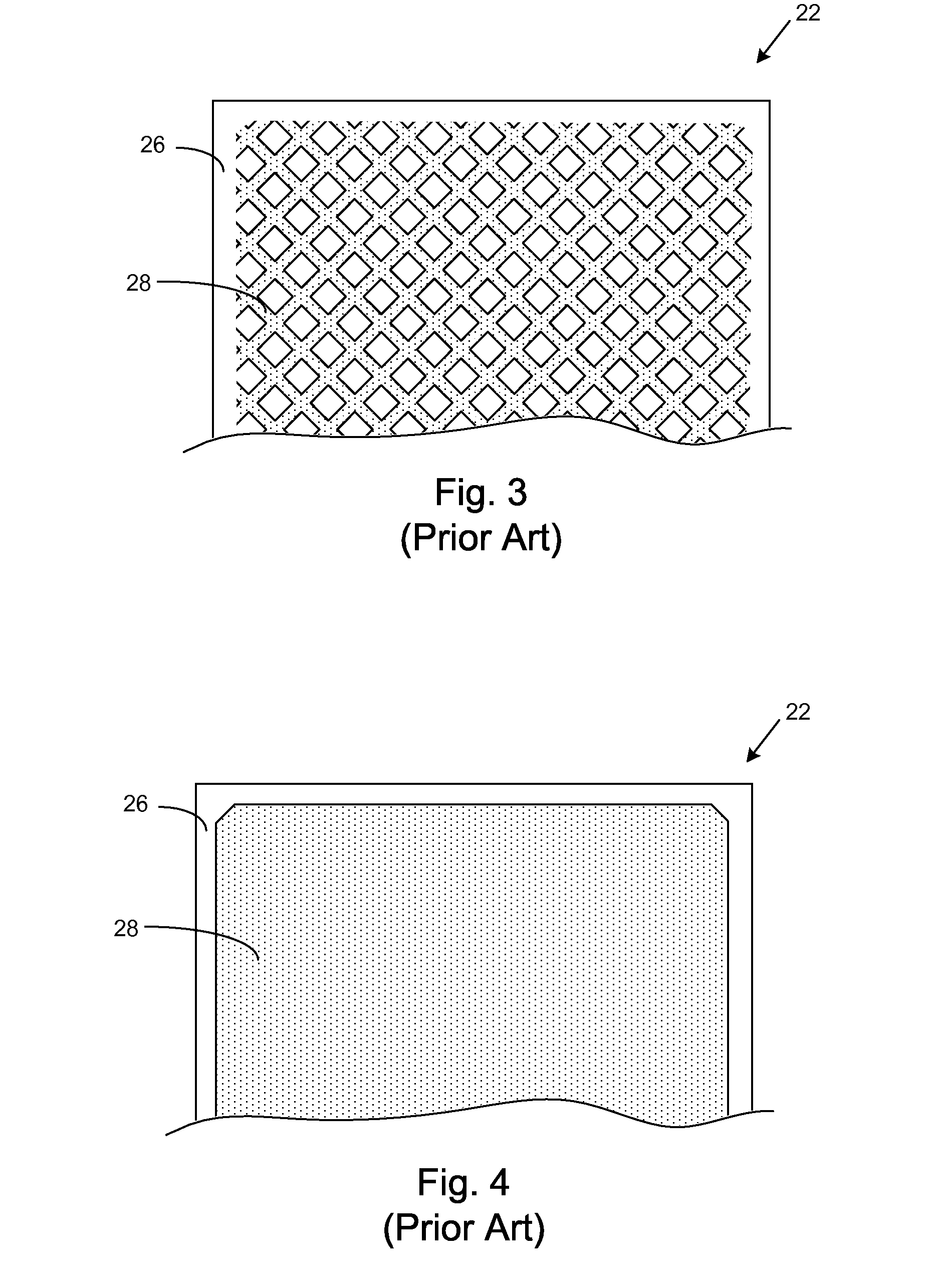
However, owing to differences in thermal expansion coefficients, a solid uniform layer of copper on the substrates leads to warping and other problems during the elevated temperature processes during package formation.
Moreover, with thin semiconductor die, die cracking occurs at unacceptably high rates during the molding process with either one of the patterns shown in FIGS. 3 and 4.

Method used


Image

  • Rigid wave pattern design on chip carrier substrate and printed circuit board for semiconductor and electronic sub-system packaging
  • Rigid wave pattern design on chip carrier substrate and printed circuit board for semiconductor and electronic sub-system packaging
  • Rigid wave pattern design on chip carrier substrate and printed circuit board for semiconductor and electronic sub-system packaging

Examples


Embodiment Construction

[0033] Embodiments of the invention will now be described with reference to FIGS. 5 through 18, which relate to a strengthened semiconductor package. It is understood that the present invention may be embodied in many different forms and should not be construed as being limited to the embodiments set forth herein. Rather, these embodiments are provided so that this disclosure will be thorough and complete and will fully convey the invention to those skilled in the art. Indeed, the invention is intended to cover alternatives, modifications and equivalents of these embodiments, which are included within the scope and spirit of the invention as defined by the appended claims. Furthermore, in the following detailed description of the present invention, numerous specific details are set forth in order to provide a thorough understanding of the present invention. However, it will be clear to those of ordinary skill in the art that the present invention may be practiced without such specif...


PUM


Abstract

A rigid wave pattern formed on a first side of a substrate in a semiconductor die package. The rigid wave pattern aligns with and overlies the contact fingers formed on the second side of the substrate. When the substrate and dice are encased during the molding process, the rigid wave pattern effectively reduces deformation of and stresses on the dice, therefore substantially alleviating die cracking.

Description

PRIORITY DATA [0001] This application is a continuation of U.S. patent application Ser. No. 11 / 106,699, entitled “Rigid Wave Pattern Design On Chip Carrier Substrate And Printed Circuit Board For Semiconductor And Electronic Sub-System Packaging,” filed Apr. 14, 2005 (Attorney Docket No. SAND-01061US0), now pending.BACKGROUND OF THE INVENTION [0002] 1. Field of the Invention [0003] Embodiments of the present invention relate to a method of forming a chip carrier substrate to alleviate chip cracking, and a chip carrier formed thereby. [0004] 2. Description of the Related Art [0005] The strong growth in demand for portable consumer electronics is driving the need for high-capacity storage devices. Non-volatile semiconductor memory devices, such as flash memory storage cards, are becoming widely used to meet the ever-growing demands on digital information storage and exchange. Their portability, versatility and rugged design, along with their high reliability and large capacity, have m...

Claims


Application Information

Patent Timeline
Patent Type & Authority Applications(United States)
IPC IPC(8): H01L23/12H01L21/00
CPCH01L23/3121H01L2224/06151H01L23/49838H01L2224/32057H01L2224/32225H01L2224/48091H01L2224/48227H01L2224/73265H01L2224/83385H01L2924/01004H01L2924/0102H01L2924/01078H01L2924/01079H01L2924/1433H01L2924/30107H01L23/49822H01L23/562H01L24/06H01L2224/05015H01L2224/05023H01L2224/0605H01L2924/15333H01L2924/01029H01L2924/1438H01L2924/15313H01L2924/15323H01L23/3114H01L24/48H01L2924/01322H01L23/48H01L2924/10253H01L2924/00014H01L2924/00H01L2924/00012H01L2924/181H01L24/73H01L2924/14H01L2224/45099H01L2224/45015H01L2924/207H01L23/498H01L24/05H01L23/49805H01L24/33H01L24/32H01L21/56H01L23/528
Inventor CHIU, CHIN-TIENLIAO, CHIH-CHINWANG, KEN JIAN MINGCHEN, HAN-SHIAOYU, CHEEMENTAKIAR, HEM
Owner SANDISK TECH LLC
Learn More