Semiconductor device

a technology of infrared imaging and semiconductors, applied in the field of semiconductor devices, can solve the problems of increasing circuit area and power consumption, and achieve the effects of reducing the noise of the operational amplifier, reducing the effect of 1/f noise, and large area of the operational amplifier

Active Publication Date: 2008-02-28
RENESAS ELECTRONICS CORP
View PDF4 Cites 11 Cited by
  • Summary
  • Abstract
  • Description
  • Claims
  • Application Information

AI Technical Summary

Benefits of technology

[0029]Meanwhile, the variations at the inverting input terminal (−) of the integrating operational amplifier 4 may be suppressed to some extent by improving the driving capability of the integrating operational amplifier 4. However, the effect achieved is relatively small.
[0055]According to the present invention, in which the input voltage is received by the source follower, it is possible to achieve the function of reducing drift, preventing high temperature spurious signal and lowering noise with small circuit area and low power consumption.

Problems solved by technology

In the above-described configurations, there is a problem of increase both in circuit area and in power consumption in order to reduce noise.

Method used


Image

  • Semiconductor device
  • Semiconductor device
  • Semiconductor device

Examples


Embodiment Construction

OF THE INVENTION

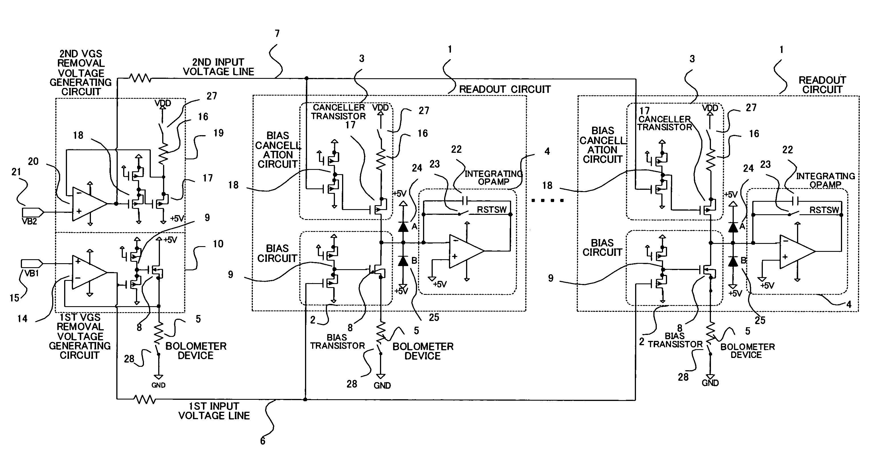
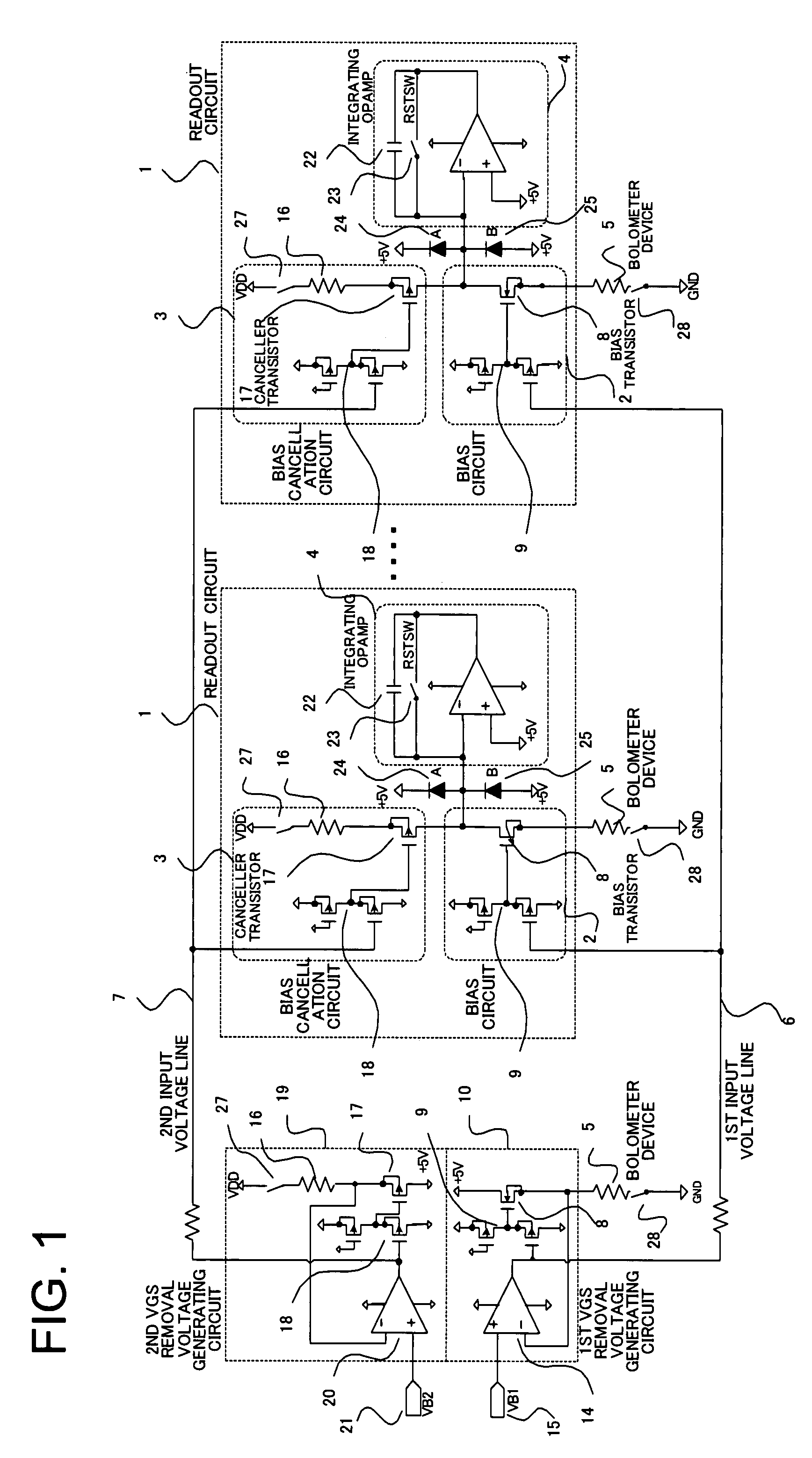
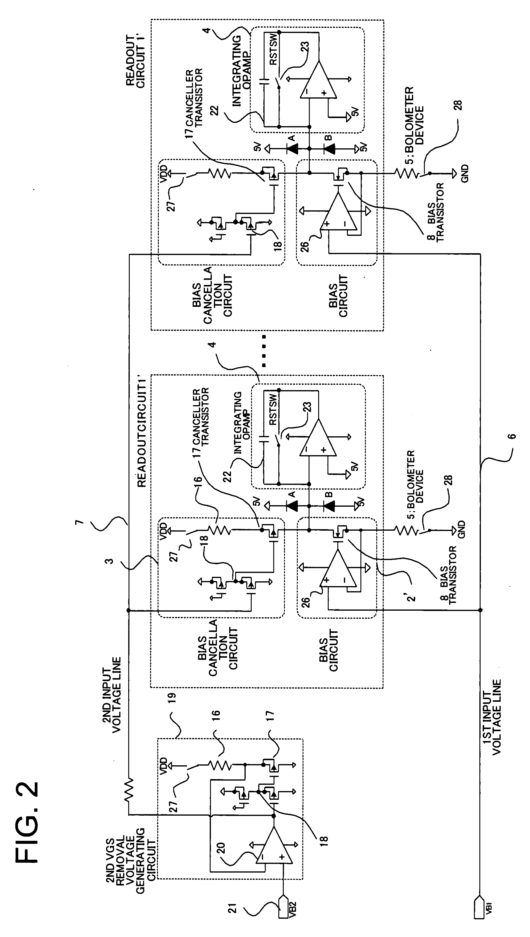
[0063]The present invention will now be described with reference to the accompanying drawings. In one mode according to the present invention, as shown in FIG. 1, there are provided a plural number of readout circuits each including a bias circuit 2, a bias cancellation circuit 3 and an integrating operational amplifier (integrator) 4. The bias circuit has a bias transistor 8 for supplying the constant voltage to a bolometer device 5, and the bias cancellation circuit has a canceller transistor 17 for removing an offset component of the current flowing in the bolometer device. The integrating operational amplifier (integrator) 4 integrates the difference current flowing through the bias and canceller transistors. The bias circuit 2 includes a first source follower circuit 9 receiving the voltage on the first input voltage line 6 to supply the output voltage to the gate of the bias transistor 8. The bias cancellation circuit 3 includes a second source follower circuit...


PUM


Abstract

Disclosed is a bolometer infrared imaging device including a plural number of readout circuits, each comprising a bias circuit that includes a bias transistor that supplies a constant voltage to a bolometer device, a bias cancellation circuit that includes a canceller transistor that removes offset current component of the bolometer device and an integrating operational amplifier that integrates the difference current between the current flowing in the bias transistor and that flowing in the canceller transistor. The bias circuit includes a source follower circuit that receives a first input voltage and supplies an output voltage to the gate of the bias transistor. The bias cancellation circuit includes a source follower circuit that receives a second input voltage and supplies an output voltage to the gate of the canceller transistor.

Description

RELATED APPLICATION[0001]This application is based upon and claims the benefit of the priority of Japanese patent application No. 2006-194337, filed on Jul. 14, 2006, the disclosure of which is incorporated herein in its entirety by reference thereto.FIELD OF THE INVENTION[0002]This invention relates to a semiconductor device. More particularly, it relates to a bolometer-type infrared imaging apparatus which includes a one-dimensional or two-dimensional sensor array and a readout circuit.BACKGROUND OF THE INVENTION[0003]In a bolometer-type infrared imaging apparatus, infrared signals are extremely low in level. Hence, in a readout circuit, variances other than infrared signals need to be suppressed. Among the important items of characteristics of the readout circuit, there are a circuit noise, a high temperature spurious signal and temperature drift of the circuit. It is noted that smaller the values of these characteristics are desirable to improve characteristics of the readout ci...

Claims


Application Information

Patent Timeline
Patent Type & Authority Applications(United States)
IPC IPC(8): G05F1/10G01J1/42H01L27/14H04N25/00
CPCG01J5/22G05F1/46H04N5/378H04N5/357H04N5/359H04N5/33H04N25/671H04N25/76H04N25/78H04N25/21H04N25/622H04N25/60H04N25/62H04N25/75
Inventor KAWANO, KATSUYA
Owner RENESAS ELECTRONICS CORP
Why Eureka
Try Eureka