
Semiconductor device contact resistant to deterioration due to heat and method for manufacturing contact

a semiconductor device and heat treatment technology, applied in the field of contact, can solve the problems of contact being removed, contact being also removed, and the inability to form shape memory alloys by plating, etc., and achieve the effects of improving the electrical conductivity of the contact, excellent shape recovery properties, and large elastic for

Inactive Publication Date: 2008-02-07
ALPS ALPINE CO LTD
View PDF52 Cites 77 Cited by
  • Summary
  • Abstract
  • Description
  • Claims
  • Application Information

AI Technical Summary

Benefits of technology

[0011]Furthermore, the present invention provides a method for manufacturing a contact capable of preventing permanent set thereof due to repetition of a burn-in test.
[0041]According to the method for manufacturing a contact of the present invention, the contact is formed by laminating the shape memory alloy film having an excellent shape recovery property on the surface of the metal spring film having a predetermined film thickness, and the shape memory alloy film is patterned by using the sacrificial metal film having the excellent heat resistance. Therefore, an effect of producing a contact, which does not cause permanent set even when the burn-in test is repeated, can be exerted.

Problems solved by technology

Therefore, when the burn-in test is repeated, slip deformation which becomes a cause of permanent deformation tends to occur.
Consequently, there is a problem in that the permanent set in the shape of the contact occurs in a direction in which an appropriate pressure is not applied to the bump.
However, the shape memory alloy cannot be formed by plating.
Although a shape memory alloy film can be formed by sputtering the shape memory alloy, when etching is performed to obtain a desired shape after the sputtering is performed, since the etching resistance of the material for the contact is low with respect to the etching solution of the shape memory alloy, there is a disadvantage that the contact is also removed by etching during the etching of the shape memory alloy.
Furthermore, when lift-off by using a resist is intended, sputtering and a heat treatment of the shape memory alloy must be performed under a high temperature environment at about 200° C. to 500° C. Consequently, even when patterning is performed by using an organic resist material, a contact having a desired shape cannot be obtained because the organic resist material cannot endure the high temperature environment.

Method used


Image

  • Semiconductor device contact resistant to deterioration due to heat and method for manufacturing contact
  • Semiconductor device contact resistant to deterioration due to heat and method for manufacturing contact
  • Semiconductor device contact resistant to deterioration due to heat and method for manufacturing contact

Examples


Embodiment Construction

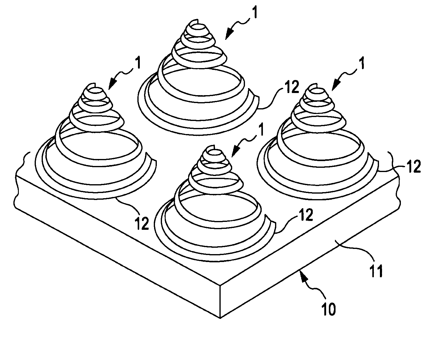
[0051]A contact according to an embodiment of the present invention will be described below with reference to FIG. 1 and FIG. 2.

[0052]FIG. 1 is a perspective view showing a contact 1 of the present embodiment. FIG. 2 is a vertical sectional view showing the contact 1 of the present embodiment. As shown in FIG. 1, the contact 1 of the present embodiment is formed into the shape of a conical spiral, in which the center portion serves as a top portion, and is connected to a connection terminal 12 disposed on an insulating substrate 11 of a probe card (inspection wiring board) 10. As shown in FIG. 2, this contact 1 is formed by laminating a metal spring film 2 and a shape memory alloy film 3. Furthermore, the contact 1 of the present embodiment is formed by laminating a seed film 4, an auxiliary electrically conductive film 5, and an electrically conductive film 6 at their respective predetermined locations as auxiliary films of the metal spring film 2 and the shape memory alloy film 3....


PUM


Abstract

A Contact according to an aspect of the present invention is formed by laminating a shape memory alloy film on a surface of a metal spring film, and the shape thereof is a conical spiral. A manufacturing method therefor is composed of 11 steps including a step of preparing a sacrificial metal film, a step of forming a resist cone, a step of patterning a resist film, a step of preparing a shape memory alloy film, and the like. Since an organic resist material has poor heat resistance, the sacrificial metal film is formed in advance, the resist is removed before sputtering of the shape memory alloy film, the sacrificial metal film is removed after sputtering of a shape memory alloy and a heat treatment, which are performed at high temperatures, so as to lift off an excess shape memory alloy film.

Description

CLAIM OF PRIORITY[0001]This application claims benefit of the Japanese Patent Application No. 2006-211791 filed on Aug. 3, 2006, which is hereby incorporated by reference.BACKGROUND OF THE INVENTION[0002]1. Field of the Invention[0003]The present invention relates to a contact and a method for manufacturing the contact. In particular, the present invention relates to a contact suitable for use in electrical connection to a semiconductor device having bumps (protrusion electrodes) formed into the shape of a sphere or a land, as well as a method for manufacturing the contact.[0004]2. Description of the Related Art[0005]In general, in a manufacturing process of a semiconductor device, e.g., an integrated circuit (IC) or large scale integration (LSI: IC in which the degree of integration of elements is 1,000 to 10,000), a produced semiconductor device is connected to an inspection wiring board called a probe card and thereby, the semiconductor device is subjected to an electric signal i...

Claims


Application Information

Patent Timeline
IPC IPC(8): H01R12/00
CPCG01R1/06733G01R1/06755G01R31/2863H01R4/01H01R12/57H01R13/03H01R13/2421H01R12/718H01L2924/00013H01L2224/13099H01L2224/13599H01L2224/05599H01L2224/05099H01L2224/29099H01L2224/29599
Inventor MURATA, SHINJI
Owner ALPS ALPINE CO LTD
Learn More