Optical Film, Producing Method Therefor, Polarizing Plate and Image Display Apparatus
a technology of optical film and polarizing plate, which is applied in the direction of instruments, polarising elements, cellulosic plastic layered products, etc., can solve the problems of increasing cost and deteriorating the scratch resistance of optical film
- Summary
- Abstract
- Description
- Claims
- Application Information
AI Technical Summary
Benefits of technology
Problems solved by technology
Method used
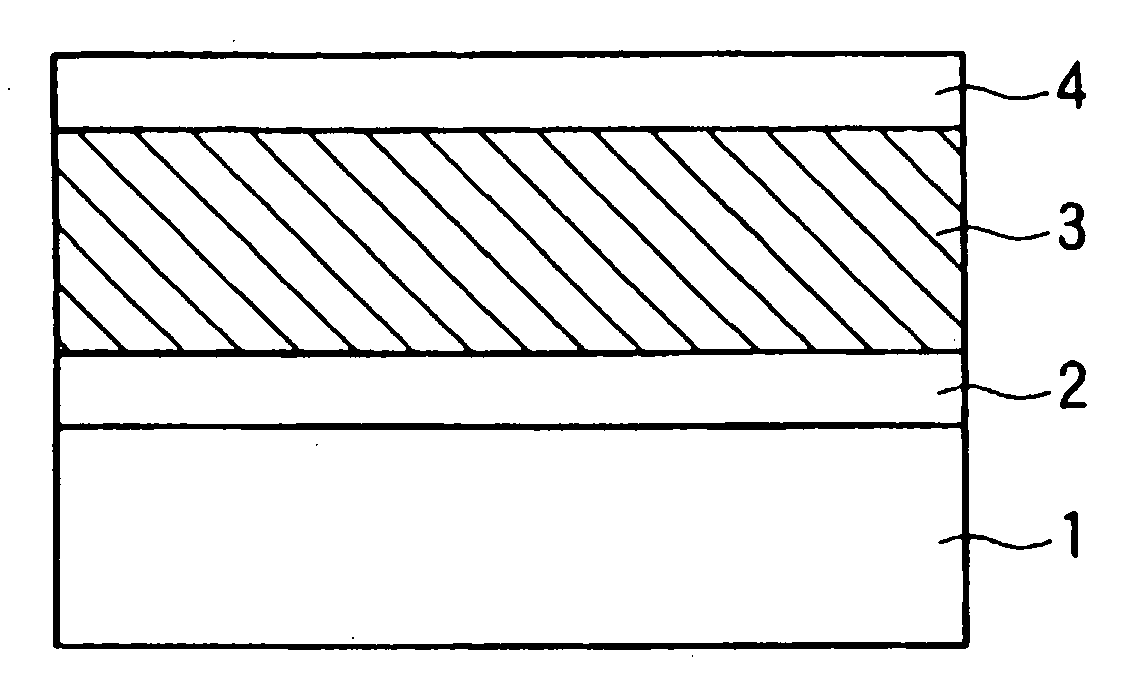
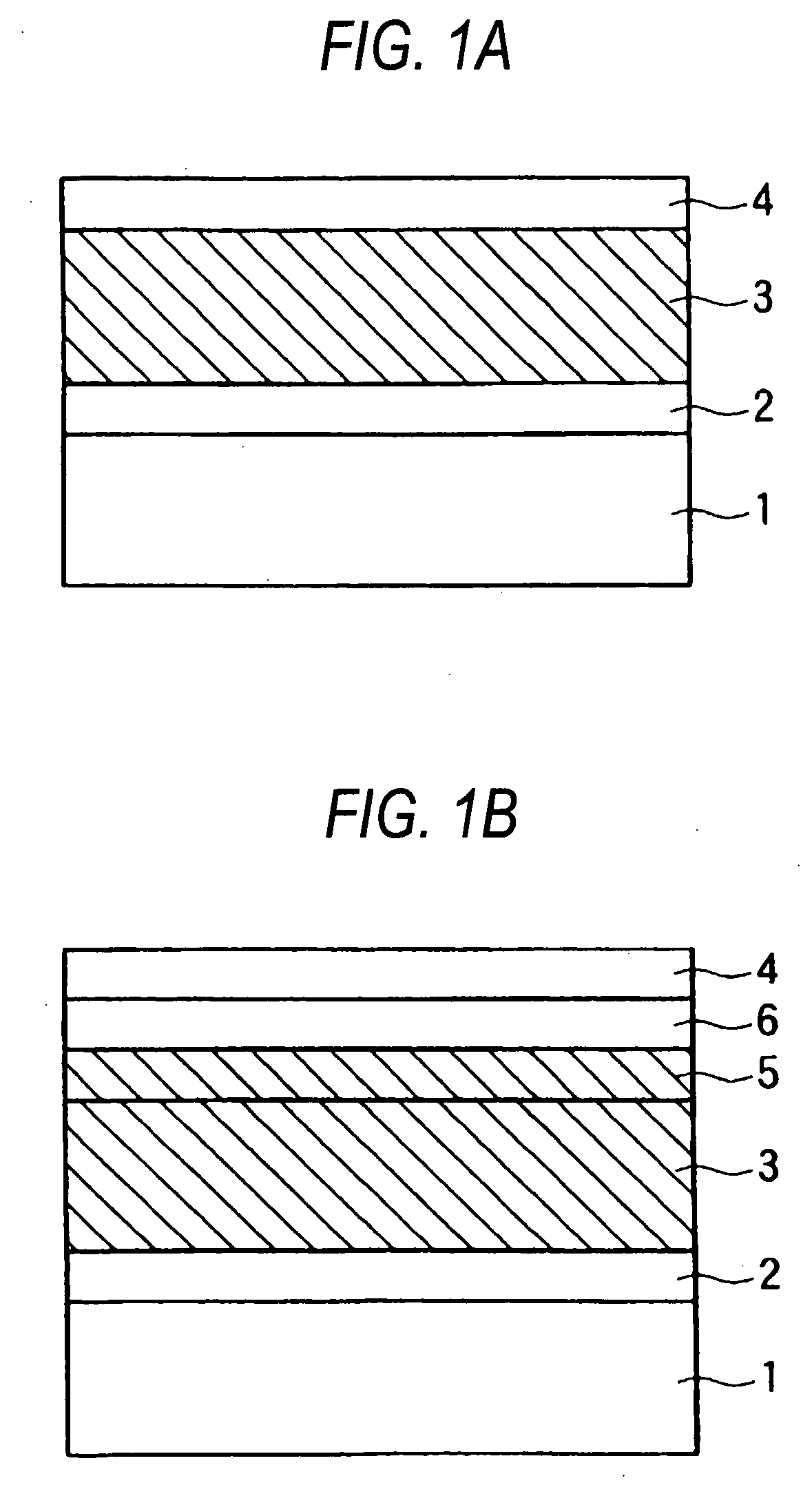
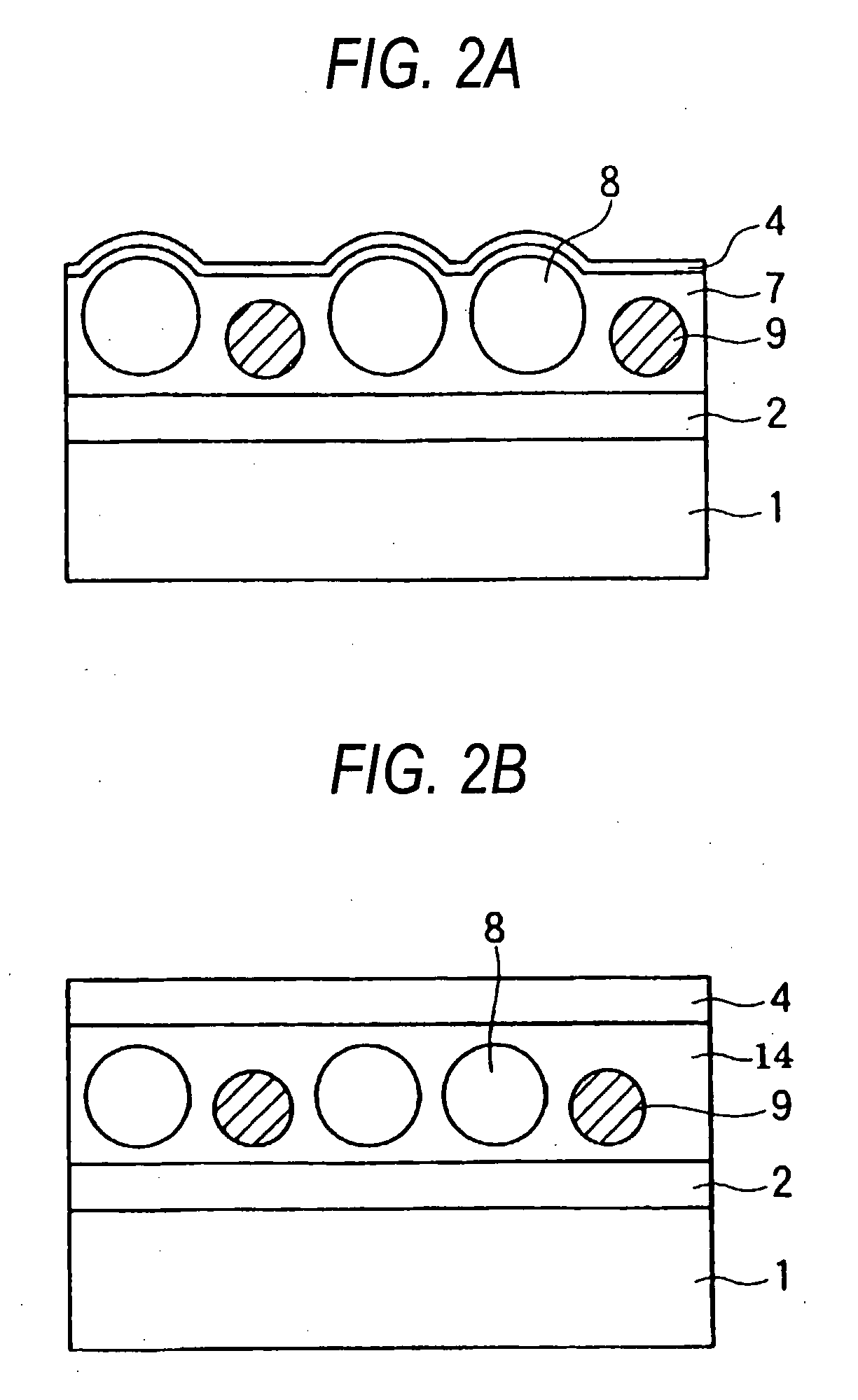
Image

Examples
example 1
[0416] In the following, the present invention will be clarified further by examples, but the present invention should not be construed as restricted by these examples.
[0417] (Antistatic Layer Coating Liquid (A))
[0418] In 12.58 parts by mass of methyl ethyl ketone, 42.50 parts by mass of cyclohexanone and 2.17 parts by mass of cellulose acetate (acetyl group substitution degree: 2.4, polymerization degree: 180) were added and agitated to obtain a cellulose acetate solution.
[0419] In the cellulose acetate solution, 42.75 parts by mass of a commercially available dispersion of antimony-containing tin oxide (ATO) (SNS-10M, solid concentration 30 mass %, manufactured by Ishihara Sangyo Co.) were added and agitated. The SNS-10M is a dispersion in methyl ethyl ketone (MEK), prepared by dispersing, with a dispersing agent, SN-100P (ATO, specific surface area: 80 m2 / g, manufactured by Ishihara Sangyo Co.), which is surface treated with a coupling agent.
[0420] The solution was filtered w...
example 1-1
[0474] On a triacetyl cellulose film of a thickness of 80 μm and a width of 1340 mm (TAC-TD80U, manufactured by Fuji Photo Film Co., Ltd.), the aforementioned antistatic layer coating liquid (A) was coated with a die coating method. It was dried for 150 seconds at 100° C. to obtain an antistatic layer of a thickness of 0.2 μm. Then, on the antistatic layer, the hard coat layer coating liquid (I) was coated by a die coating method. After drying for 150 seconds at 100° C., the coated layer was cured, under a nitrogen purging (oxygen concentration of 0.1% or less), by an ultraviolet irradiation of an irradiation intensity of 400 mW / cm2 and an irradiation amount of 250 mJ / cm2 utilizing an air-cooled metal halide lamp of 160 W / cm (manufactured by Eyegraphics Co.) to obtain a hard coat layer of a thickness of 2.5 μm. In this manner an optical film of Example 1-1 was prepared.
example 1-2
[0475] An optical film of Example 1-2 was prepared in the identical manner as in Example 1-1, except that the antistatic layer coating liquid (A) was replaced by the antistatic layer coating liquid (B).
PUM
| Property | Measurement | Unit |
|---|---|---|
| Percent by mass | aaaaa | aaaaa |
| Particle size | aaaaa | aaaaa |
| Fraction | aaaaa | aaaaa |
Abstract
Description
Claims
Application Information
 - R&D
- Intellectual Property
- Life Sciences
- Materials
- Tech Scout
- Unparalleled Data Quality
- Higher Quality Content
- 60% Fewer Hallucinations
Browse by: Latest US Patents, China's latest patents, Technical Efficacy Thesaurus, Application Domain, Technology Topic, Popular Technical Reports.
© 2025 PatSnap. All rights reserved.Legal|Privacy policy|Modern Slavery Act Transparency Statement|Sitemap|About US| Contact US: help@patsnap.com