
Handler and method of testing semiconductor device by means of the handler

a technology of handler and handler, which is applied in the direction of electrical testing, measurement devices, instruments, etc., can solve the problems of increasing the number of pins, increasing the cost of semiconductor devices, and reducing the price of semiconductor devices year by year with a large drop in set prices, so as to improve test efficiency and test stability.

Inactive Publication Date: 2008-01-10
PANASONIC CORP
View PDF6 Cites 18 Cited by
  • Summary
  • Abstract
  • Description
  • Claims
  • Application Information

AI Technical Summary

Benefits of technology

[0008]In the handler 407, the semiconductor devices 403a and 403b are simultaneously set on the sockets 404a and 404b and are simultaneously removed from the sockets 404a and 404b. Thus if the semiconductor device 403a is judged as being a defective item, the semiconductor device 403a cannot be replaced with another untested device until the completion of a test on the other semiconductor device 403b, increasing the test time. Consequently, the test efficiency decreases.
[0009]The present invention is designed to solve the aforementioned conventional problem. An object of the present invention is to provide a handler and a testing method thereof which enable efficient measurements on a plurality of semiconductor devices.
[0021]According to this configuration, even when a “defective item” is found among semiconductor devices to be tested, processing on the defective item can be performed for each measurement part. The defective item can be replaced with another untested semiconductor device and the subsequent semiconductor device can be tested at the occurrence of the defect, so that test efficiency improves. Further, it is possible to control the contact pressure and the contact pressing speed of each measurement part based on a test result for each measurement part, so that the optimum contact pressure and contact pressing speed can be set for each measurement part and a test can be more stable.

Problems solved by technology

In recent years, semiconductor devices have become complicated, the number of pins has increased, and a test time has also increased with the progress of semiconductor-related technology.
On the other hand, the prices of semiconductor devices have considerably decreased year by year with a large drop in set prices.

Method used


Image

  • Handler and method of testing semiconductor device by means of the handler
  • Handler and method of testing semiconductor device by means of the handler
  • Handler and method of testing semiconductor device by means of the handler

Examples


first embodiment

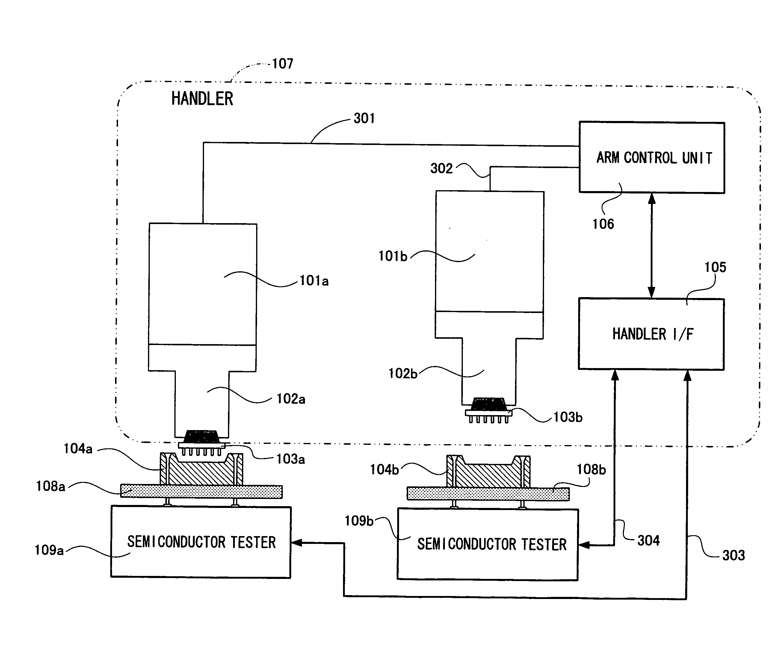
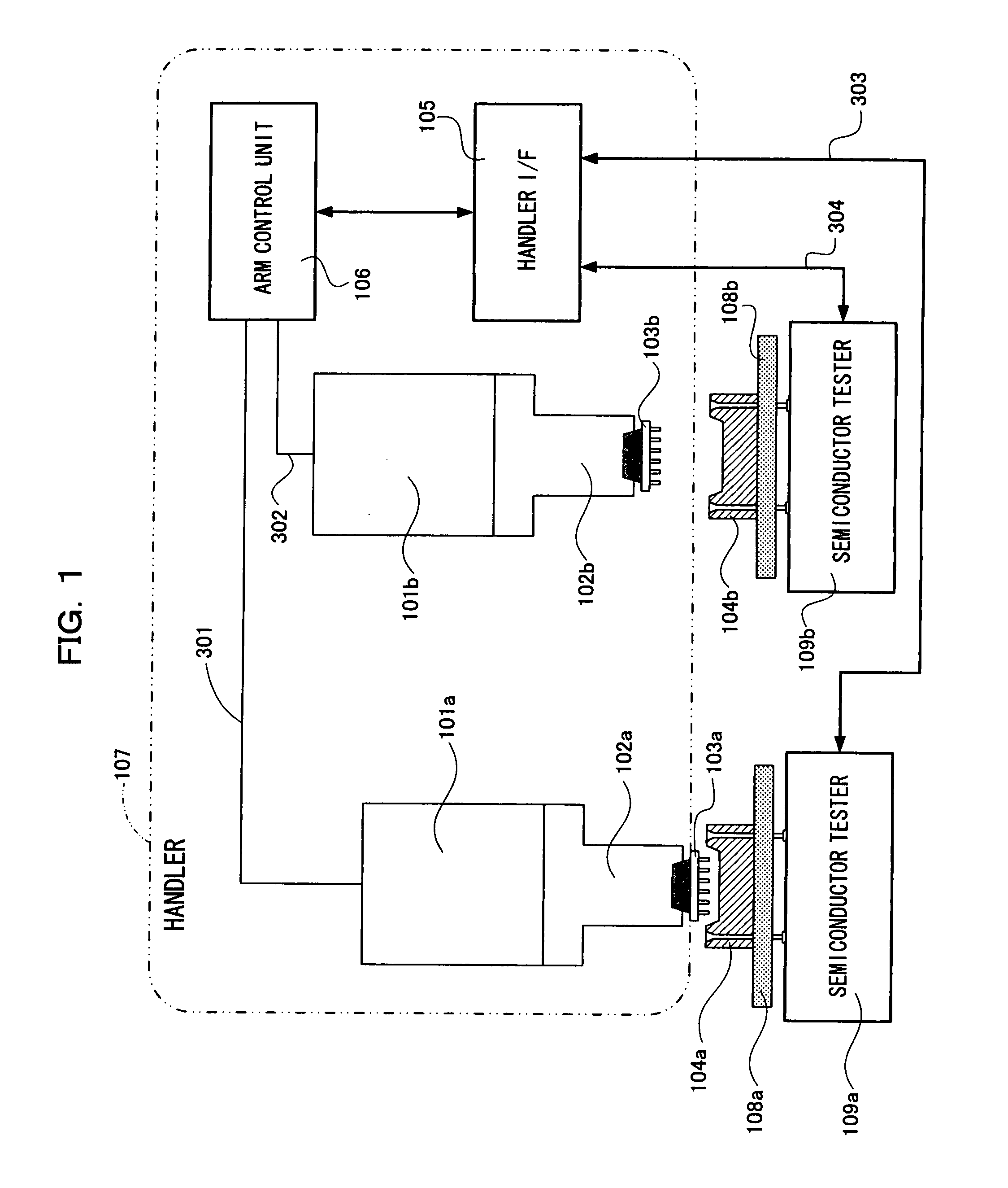
[0028]FIG. 1 shows a handler of First Embodiment.

[0029]A handler 107 is made up of two contact arms 101a and 101b, contact pushers 102a and 102b which are attached to the ends of the contact arms 101a and 101b and can hold semiconductor devices 103a and 103b, an arm control unit 106 for controlling the operations of the contact arms 101a and 101b, and a handler interface 105 for converting signals and transferring information between the arm control unit 106 and semiconductor testers 109a and 109b.

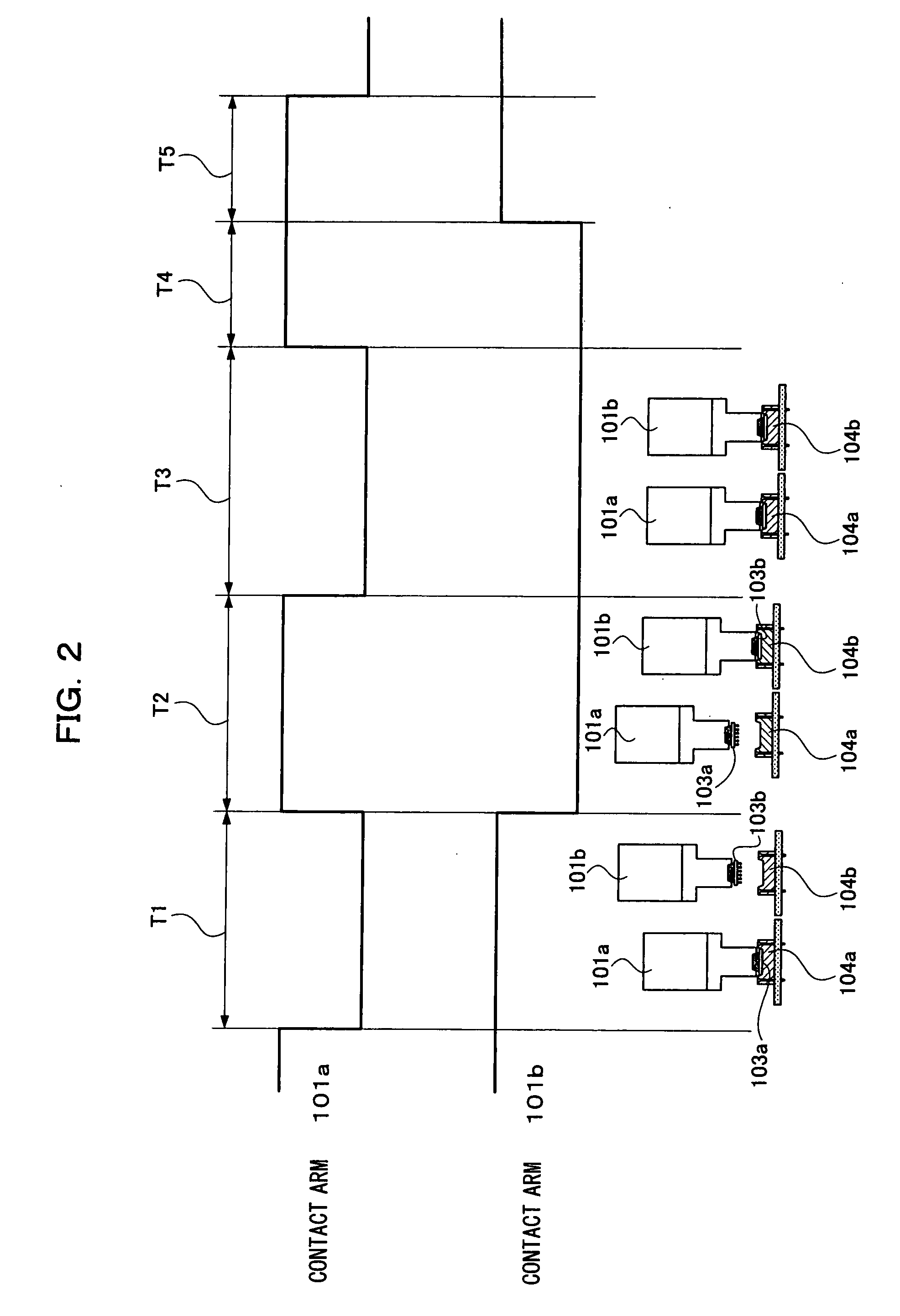
[0030]The arm control unit 106 separately supplies operation signals to the contact arms 101a and 101b through signal lines 301 and 302 and performs contact control such that the semiconductor devices 103a and 103b to be tested are contacted to a socket 104a on a test board 108a electrically connected to the semiconductor tester 109a and a socket 104b on a test board 18b electrically connected to the semiconductor tester 109b. At this moment, the arm control unit 106 controls the timing o...

second embodiment

[0039]The following is a specific example in which an arm control unit 106 controls the timing of control for each of contact arms 101a and 101b according to First Embodiment.

[0040]Second Embodiment describes an example in which the controlled variables of contact arms 101a and 101b are set by the arm control unit 106 from semiconductor testers 109a and 109b through a handler interface 105. In this example, as a controlled variable of the arm, the temperature of a contact is calibrated during a test.

[0041]Contact pushers 102a and 102b include heaters serving as heating devices. The temperature of the contact pusher 102a is adjusted to a target temperature by the arm control unit 106 through the contact arm 101a. The temperature of the contact pusher 102b is adjusted to the target temperature by the arm control unit 106 through the contact arm 101b.

[0042]When semiconductor devices are tested at a high temperature, in order to more accurately set the temperature of each measurement p...

third embodiment

[0046]FIGS. 3 and 4 show Third Embodiment of the present invention.

[0047]First Embodiment shown in FIG. 1 described the testing method in which the test boards 108a and 108b are electrically connected to the respective semiconductor testers 109a and 109b, and the semiconductor testers 109a and 109b are connected to the handler 107 via signal lines 303 and 304 to transmit and receive signals, so that a test is conducted. In FIG. 3, the handler 107 of First Embodiment is used and a test is conducted using a test board 208 of FIG. 4 instead of the test boards 108a and 108b.

[0048]In FIG. 3, although the handler 107 is identical to that of FIG. 1, the test board 208 is electrically connected to a single semiconductor tester 209 and the semiconductor tester 209 is connected to the handler 107 via a signal line 305 to transmit and receive signals.

[0049]As shown in FIG. 4, the signal line 305 has signal lines 301 which directly branch to share power supply wiring, ground wiring and the lik...


PUM


Abstract

An object of the present invention is to provide a handler and a testing method thereof which enable efficient measurements on a plurality of semiconductor devices. An arm control unit 106 controls, for each of contact arms 101a and 101b, the timing of control for performing contact control for bringing semiconductor devices 103a and 103b to be tested to one of a contact state and a non-contact state with test boards 108a and 108b connected to semiconductor testers 109a and 109b. The plurality of semiconductor devices are simultaneously measured using the handler 107, so that when a “defective item” is found on a specific measurement part, only the defective item on the measurement part can be replaced with another untested item and thus tests can be efficiently conducted.

Description

FIELD OF THE INVENTION [0001]The present invention relates to a handler for transporting and contacting a semiconductor device to be tested to a socket on a test board connected to a semiconductor tester, and transporting the tested semiconductor device to one of a conforming item tray and a non-conforming item tray according to the test result.BACKGROUND OF THE INVENTION [0002]In recent years, semiconductor devices have become complicated, the number of pins has increased, and a test time has also increased with the progress of semiconductor-related technology. On the other hand, the prices of semiconductor devices have considerably decreased year by year with a large drop in set prices. Under these circumstances, in order to also reduce test costs in tests on semiconductor devices, it is strongly desired to efficiently test semiconductor devices by connecting a plurality of semiconductor devices to a semiconductor tester. Such a tester is described in Japanese Patent Publication N...

Claims


Application Information

Patent Timeline
Patent Type & Authority Applications(United States)
IPC IPC(8): G01R31/26
CPCG01R31/2893
Inventor NAKASE, MASAYUKIAKAHORI, KOUJIKANEMITSU, TOMOHIKOKAMATANI, YASUHIRO
Owner PANASONIC CORP
Learn More