
Light-emitting element, light-emitting device and an electronic device

a technology of light-emitting elements and electronic devices, which is applied in the direction of thermoelectric device junction materials, semiconductor devices, electrical devices, etc., can solve the problems of difficult to obtain features and short lifetime, and achieve the effect of longer lifetimes

Active Publication Date: 2008-01-10
SEMICON ENERGY LAB CO LTD
View PDF32 Cites 36 Cited by
  • Summary
  • Abstract
  • Description
  • Claims
  • Application Information

AI Technical Summary

Benefits of technology

The present invention is a light-emitting element that includes a plurality of layers between a pair of electrodes. The layers include an EL layer that can be made of different materials and can have different functions. The invention provides various modes for the light-emitting element, including a mode where the layers are simply mixed and charged materials are transferred between them. The light-emitting element can be used in various applications, such as displays and lighting. The invention also provides a method for forming the light-emitting element by sequentially stacking layers. The layers can be made of conductive materials, such as metal or conductive compounds, or can be formed using a sol-gel method. The invention allows for the use of different materials and combinations of layers to create the EL layer, providing flexibility in design.

Problems solved by technology

This is a feature which is difficult to be obtained by point light sources typified by an incandescent lamp and an LED or linear light sources typified by a fluorescent lamp.
Such a light-emitting element including a light-emitting organic compound can be driven at lower voltage than a light-emitting element using an inorganic compound; however, such a light-emitting element including a light-emitting organic compound has a problem in that its lifetime is short.

Method used


Image

  • Light-emitting element, light-emitting device and an electronic device
  • Light-emitting element, light-emitting device and an electronic device
  • Light-emitting element, light-emitting device and an electronic device

Examples


example 1

Measurement Example 1

DPAnth

[0169]In this measurement example 1, the oxidative reaction characteristic and the reductive reaction characteristic of DPAnth were measured by a cyclicvoltammetry (CV) measurement. The scan speed was 0.1 V / sec and 100 cycles of measurement was conducted.

[0170]Firstly, FIG. 16A shows a measurement result of the oxidative reaction characteristic. In the measurement of the oxidative reaction characteristic, the potential of a working electrode with respect to the reference electrode was scanned from −0.05 to 1.20 V, and then from 1.20 V to −0.05 V, which was one cycle.

[0171]As shown in FIG. 16A, the oxidation peak potential Epa remained at 0.93V without changing before (initial state) and after the 100 cycles. In addition, the current amount (oxidation peak current Ipa) in the oxidation peak potential was −11.9 μA in the initial state and −8.49 μA after the 100 cycles. Even after 100 cycles, 71% of that in the initial state was kept. Thus, it can be said tha...

example 2

Measurement Example 2

CzPA

[0176]In Measurement Example 2, the oxidative reaction characteristic and the reductive reaction characteristic of CzPA were measured by a cyclicvoltammetry (CV) measurement. The scan speed was 0.1 V / sec and 100 cycles of measurement was conducted.

[0177]Firstly, FIG. 18A shows a measurement result of the oxidative reaction characteristic. In the measurement of the oxidative reaction characteristic, the potential of the working electrode with respect to the reference electrode was scanned from −0.41 to 1.20 V, and then, from 1.20 V to −0.41 V, which was one cycle.

[0178]As shown in FIG. 18A, the oxidation peak potential Epa remained at 0.87 V without changing before (initial state) and after the 100 cycles. In addition, the current amount (oxidation peak current Ipa) in the oxidation peak potential was −12.5 μA in the initial state and −12.0 μA after the 100 cycles. Even after 100 cycles, 96% of that in the initial state was kept. Thus, it can be said that CzP...

example 3

[0184]Example 3 will specifically describe a light-emitting element of the present invention with reference to FIG. 10. Structural formulas of organic compounds used in this example are shown below.

(Light-Emitting Element 3)

[0185]First, a film of indium tin oxide containing silicon oxide was formed over a glass substrate 2101 by a sputtering method, and thus, a first electrode 2102 was formed. The thickness was 110 nm and the electrode area was 2 mm×2 mm.

[0186]Next, the substrate on which the first electrode 2102 was formed was fixed to a substrate holder that was provided in a vacuum evaporation apparatus, such that the surface on which the first electrode 2102 was formed came to the lower side. After the pressure was reduced to approximately 10−4 Pa, 4,4′-bis[N-(1-naphtyl)-N-phenylamino]biphenyl (abbreviation: NPB) and molybdenum (VI) oxide were co-evaporated on the first electrode 2102 to form a layer 2103 containing a composite material. The thickness was 50 nm, and the weight r...


PUM


Abstract

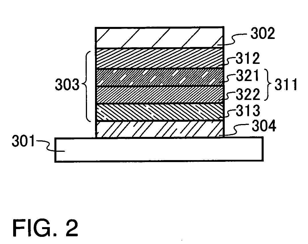
The present invention provides a light-emitting element including an electron-transporting layer and a hole-transporting layer between a first electrode and a second electrode; and a first layer and a second layer between the electron-transporting layer and the hole-transporting layer, wherein the first layer includes a first organic compound and an organic compound having a hole-transporting property, the second layer includes a second organic compound and an organic compound having an electron-transporting property, the first layer is formed in contact with the first electrode side of the second layer, the first organic compound and the second organic compound are the same compound, and a voltage is applied to the first electrode and the second electrode, so that both of the first organic compound and the second organic compound emit light.

Description

TECHNICAL FIELD[0001]The present invention relates to current excitation type light-emitting elements. Further, the present invention relates to light-emitting devices and electronic devices having the light-emitting element.BACKGROUND ART[0002]In recent years, research and development have been extensively conducted on light-emitting elements using electroluminescence. In a basic structure of such a light-emitting element, a substance having a light-emitting property is interposed between a pair of electrodes. By voltage application to this element, light emission can be obtained from the substance having a light-emitting property.[0003]Since such a light-emitting element is of self-light-emitting type, it is considered that the light-emitting element has advantages over a liquid crystal display in that visibility of pixels is high, backlight is not required, and so on and is therefore suitable as flat panel display elements. In addition, other advantages of such a light-emitting e...

Claims


Application Information

Patent Timeline
Patent Type & Authority Applications(United States)
IPC IPC(8): H01L29/08H01L35/24H01L51/00H10N10/856
CPCH01L51/5012H01L51/5072H01L51/5056H01L51/5048H10K50/14H10K50/11H10K50/15H10K50/16H10K85/615
Inventor OHSAWA, NOBUHARU
Owner SEMICON ENERGY LAB CO LTD
Learn More