Charge Monitoring Devices and Methods for Semiconductor Manufacturing

Inactive Publication Date: 2007-12-27
MACRONIX INT CO LTD
View PDF13 Cites 0 Cited by
  • Summary
  • Abstract
  • Description
  • Claims
  • Application Information

AI Technical Summary

Benefits of technology

[0012]Advantageously, the present invention provides simpler charge storage device structures for monitoring charging effect. The present invention also advantageously provides different device structures for controlling the sensibility of the charging effect.

Problems solved by technology

However, the hot hole injection causes oxide damage leading to charge loss in the high threshold cell and charge gain in the low threshold cell.
This difference in erase speed results in a large Vt distribution of the erase state, where some of the cells become hard to erase and some of them are over-erased.
Thus the target threshold Vt window is closed after many program and erase cycles and poor endurance is observed.
This phenomenon will become more serious as the technology continues scaling down.

Method used


Image

  • Charge Monitoring Devices and Methods for Semiconductor Manufacturing
  • Charge Monitoring Devices and Methods for Semiconductor Manufacturing
  • Charge Monitoring Devices and Methods for Semiconductor Manufacturing

Examples


Embodiment Construction

[0028]A description of structural embodiments and methods of the present invention is provided with reference to FIGS. 1-9. It is to be understood that there is no intention to limit the invention to the specifically disclosed embodiments, but that the invention may be practiced using other features, elements, methods and embodiments. Like elements in various embodiments are commonly referred to with like reference numerals.

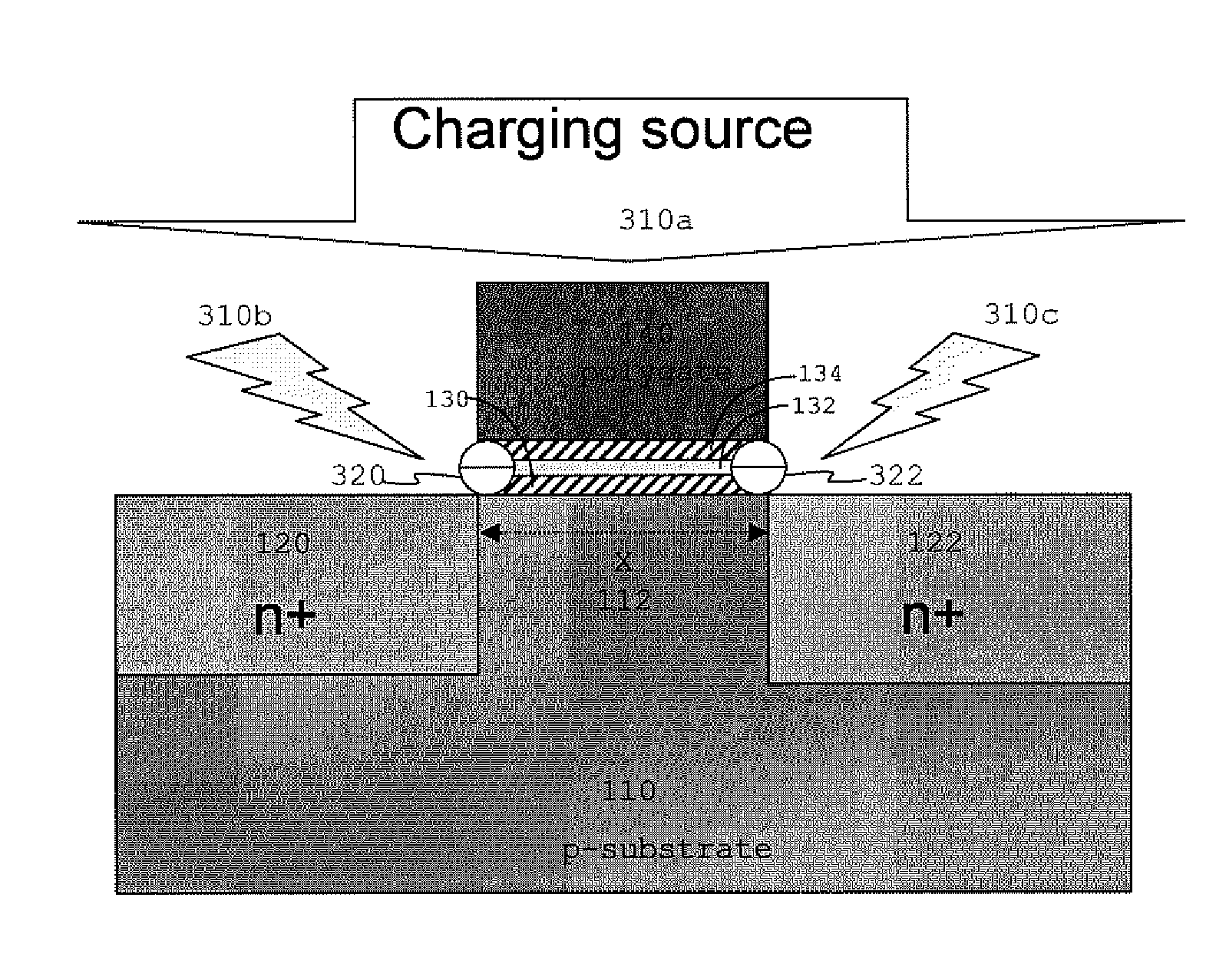
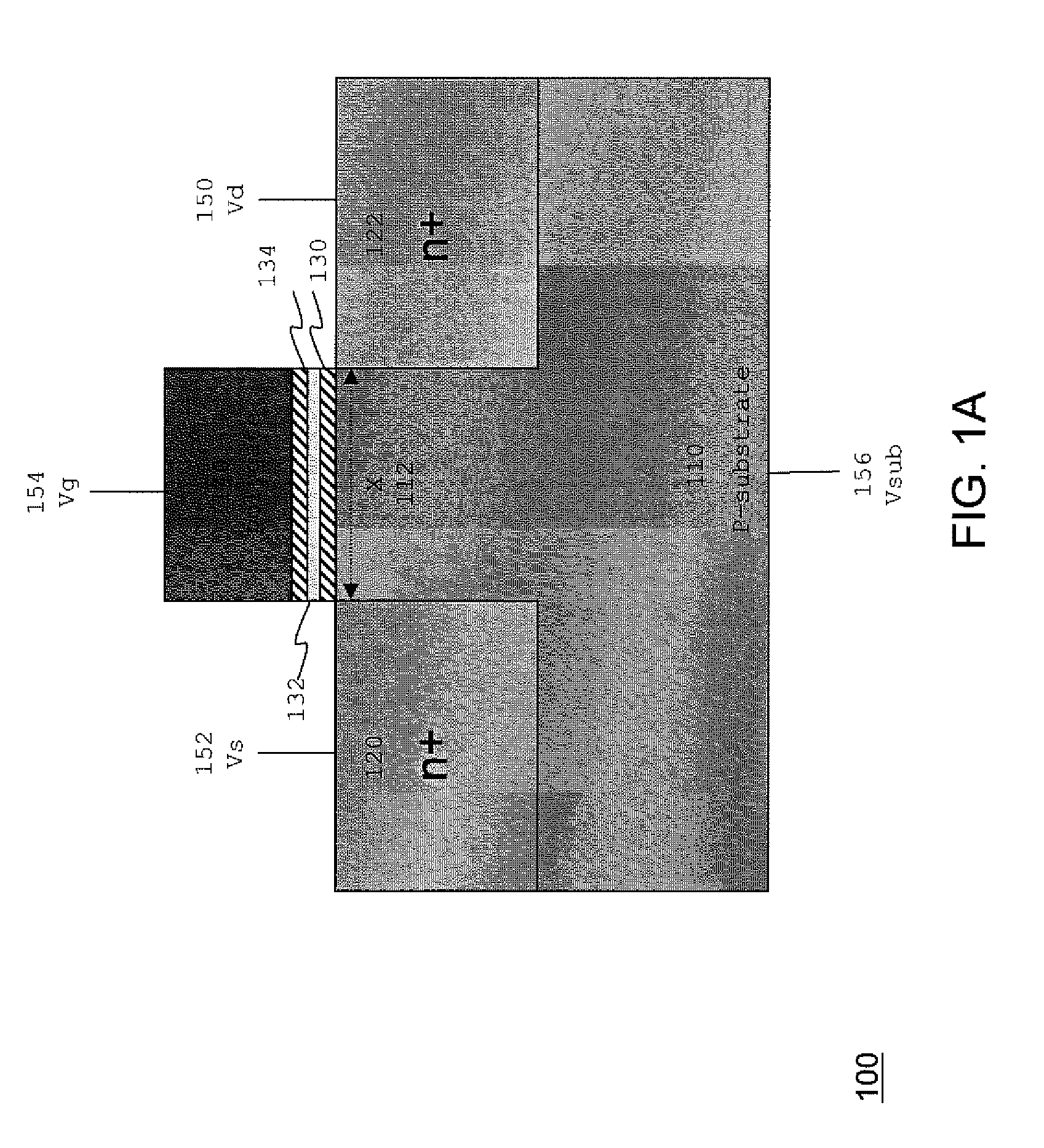
[0029]FIG. 1A is a process diagram illustrating a cross-sectional view of a CS-MOS memory structure 100. The CS-MOS memory structure 100 comprises a p-substrate 110 with n+ doped regions 120 and 122, and a p-doped region between the n+ doped regions 120 and 122. A channel width X 112 of the p-substrate 110 is positioned between the n+ doped region 120 on the left end and the n+ doped region 122 on the right end. A bottom dielectric structure 130 (bottom oxide) overlays a top surface of the channel width X 112 of the substrate 110; a charge trapping structure 132 ...


PUM


Abstract

A charge monitoring device is described for monitoring charging effect during semiconductor manufacturing. In a first aspect of the invention, a charge storage MOS memory structure comprises a substrate body, an oxide-nitride-oxide structure that overlays a top surface of the substrate and extends above the edges between a source region and a drain region, and a polygate formed over the oxide-nitride-oxide structure. When a charging source, such as UV light or plasma, is projected onto the charge storage device, the polygate of the charge storage device protects the nitride layer from charging effect The light source charges side walls of the oxide-nitride-oxide structure.

Description

BACKGROUND OF THE INVENTION[0001]1. Field of the Invention[0002]The present invention relates generally to electrically programmable and erasable memory and more particularly to charge storage devices for monitoring charging effect.[0003]2. Description of Related Art[0004]Electrically programmable and erasable nonvolatile memory technologies based on charge storage structures known as Electrically Erasable Programmable Read-Only Memory (EEPROM) and flash memory are used in a variety of modem applications. A flash memory is designed with an array of memory cells that can be independently programmed and read. Sense amplifiers in a flash memory are used to determine the data value or values stored in a nonvolatile memory. In a typical sensing scheme, an electrical current through the memory cell being sensed is compared to a reference current by a current sense amplifier.[0005]A number of memory cell structures are used for EEPROM and flash memory. As the dimensions of integrated circu...

Claims


Application Information

Patent Timeline
IPC IPC(8): H01L29/792
CPCH01L29/7923H01L29/66833
Inventor WU, CHAO-ILEE, MING HSIU
Owner MACRONIX INT CO LTD
Why Eureka
Try Eureka