Antenna Device and Communication Apparatus

Active Publication Date: 2007-12-13
MITSUBISHI MATERIALS CORP
View PDF5 Cites 193 Cited by
  • Summary
  • Abstract
  • Description
  • Claims
  • Application Information

AI Technical Summary

Benefits of technology

[0016] The present invention is contrived in order to solve the problems, and an object of the present invention is to provide an antenna device which can be miniaturized even in a relatively low frequency band such as 400 MHz band.
[0065] According to the present invention, since the conductor pattern is formed in a meander shape, it is possible to increase a length of the conductor pattern, so that it is possible to increase a gain of the antenna device similar to the aforementioned invention. In addition, since the conductor pattern is formed on a surface of the elementary body, it is possible to easily form the conductor pattern.

Problems solved by technology

For the reason, it is difficult to apply a built-in antenna device to a practical radio apparatus in a relatively low frequency such as a band of 400 MHz.
In addition, when a conventional antenna device is applied to a low frequency band such as 800 MHz, there is a problem in that a size of the antenna device greatly increases.
For example, in an application to a low frequency band such as 800 MHz, there is a problem in that a size of the antenna device greatly increases.
In addition, Formula 1 represents that, when an antenna device having the same shape is miniaturized, a band of the antenna device is reduced, so that the radiation efficiency is reduce.
Therefore, for example, since a mobile phone having a band of 800 MHz utilizes an FDD (Frequency Division Duplex) scheme using different frequency bands for transmission and reception in Japan, it is difficult to implement a compact built-in antenna capable of covering transmission and reception bands.
In addition, in the conventional antenna device, since two loading elements are disposed in a straight line shape, when the antenna device is received in an antenna receiving portion, it protrudes into an inner portion of a case, so that an arrangement of a communication control circuit is limited.
Therefore, there is a problem in that a space factor is deteriorated.

Method used


Image

  • Antenna Device and Communication Apparatus
  • Antenna Device and Communication Apparatus
  • Antenna Device and Communication Apparatus

Examples


first example

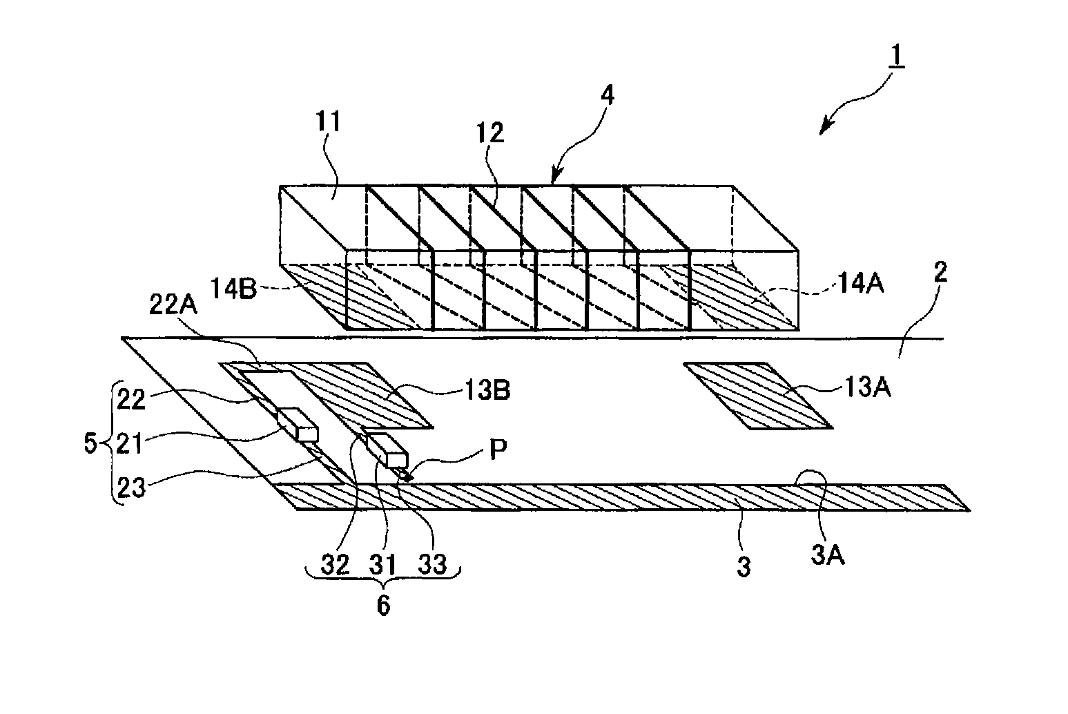
[0258] Next, first to third examples of an antenna device according to the present invention are described in detail.

[0259] As a first example, the antenna device 1 according to the first embodiment had been manufactured. As shown in FIG. 37, in the antenna device 1, the loading section 4 was made of alumina, and a copper line having a diameter p of 0.2 mm as the conductor pattern 12 had been wound around a surface of the rectangular parallelepiped elementary body 11 having a length L5 of 27 mm, a width L6 of 3.0 mm, and a thickness L7 of 1.6 mm in a helical shape with a central interval W1 of 1.5 mm.

second example

[0260] In addition, as a second example, the antenna device 50 according to the second embodiment had been manufactured.

[0261] As shown in FIG. 38, in the antenna device 50, the loading section 51 was made of alumina, and the conductor pattern 52 made of silver having a width W2 of 0.2 mm had been formed on a surface of the rectangular parallelepiped elementary body 11 having a thickness L8 of 1.0 mm in the so as for a length L9 of the elementary body 11 in the width direction thereof to be 4 mm, a length L10 of the elementary body 11 in the longitudinal direction thereof to be 4 mm, and a period to be 12 mm in a meander shape.

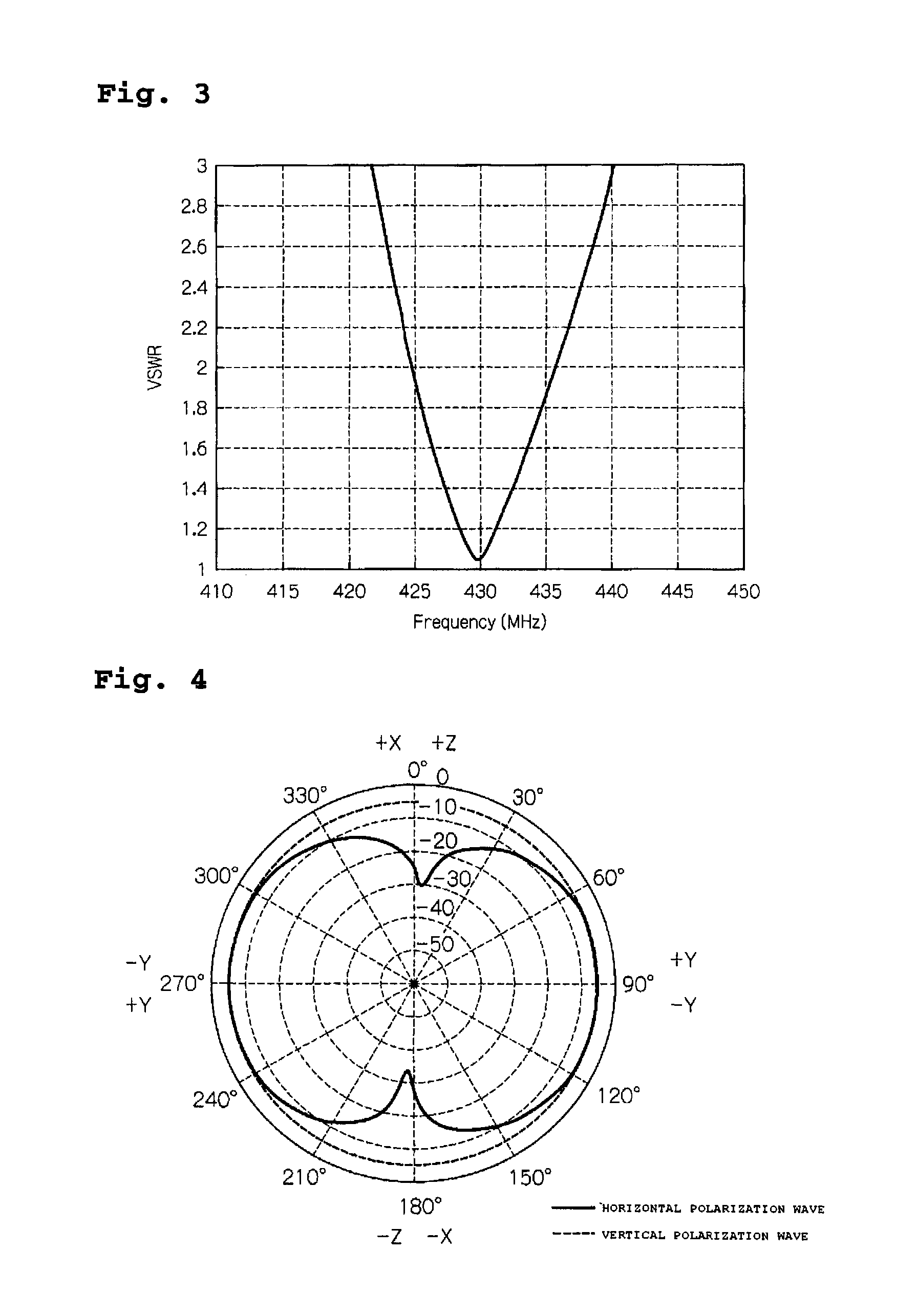
[0262] VSWR frequency characteristics of the antenna device 1 and the antenna device 50 at a frequency of from 400 to 500 MHz are shown in FIGS. 39 and 40.

[0263] As shown in FIG. 39, the antenna device 1 had a VSWR of 1.233 at a frequency of 430 MHz and a bandwidth of 18.53 MHz at a VSWR of 2.5.

[0264] In addition, as shown in FIG. 40, the antenna device 50...

third example

[0266] Next, as a third example, the antenna device 70 according to the fifth embodiment had been manufactured, and as a comparative example, an antenna device having no meander pattern 71 had been manufactured.

[0267] VSWR frequency characteristics of the antenna devices of the third example and the comparative example at a frequency of from 800 to 950 MHz are shown in FIGS. 41(a) and (b). Radiation patterns of the vertical polarization waves of the antenna devices of the third example and the comparative example are shown in FIGS. 42(a) and (b).

[0268] As shown in FIGS. 41(a) and 42(a), in the antenna device 70, a bandwidth at a VSWR of 2.0 became 38.24 MHz, and in the radiation pattern of the vertical polarization waves, a maximum value of gain became −2.43 dBd, a minimum value thereof became −4.11 dBd, and an average value thereof became −3.45 dBd.

[0269] As shown in FIGS. 41(b) and 42(b), in the antenna device of the comparative example, a bandwidth at a VSWR of 2.0 became 27.8...


PUM


Abstract

There is provided an antenna device including a substrate, an earth section which is disposed on a portion of the substrate, a feed point which is disposed on the substrate, a loading section disposed on the substrate and constructed with a line-shaped conductor pattern which is formed in a longitudinal direction of an elementary body made of a dielectric material, an inductor section which connects one end of the conductor pattern to the earth section, and a feed point which feeds a current to a connection point of the one end of the conductor pattern and the inductor section, wherein a longitudinal direction of the loading section is arranged to be parallel to an edge side of the earth section.

Description

CROSS-REFERENCE TO PRIOR APPLICATION [0001] This is a U.S. National Phase Application under 35 U.S.C. §371 of International Patent Application No. PCT / JP2004 / 019337, filed Dec. 24, 2004, and claims the benefit of Japanese Patent Application Nos. 2003-430022, filed Dec. 25, 2003; 2004-070875, filed Mar. 12, 2004; 2004-071513, filed Mar. 12, 2004; 2004-228157, filed Aug. 4, 2004; 2004-252435, filed Aug. 31, 2004 and 2004-302924, filed Oct. 18, 2004, all of which are incorporated by reference herein. The International Application was published in Japanese on Jul. 14, 2005 as International Publication No. WO 2005 / 064743 under PCT Article 21(2).TECHNICAL FIELD [0002] The present invention relates to an antenna device used for a mobile communication radio apparatus such as a mobile phone and a radio apparatus for specific low-power radio communication or weak radio communication and a communication apparatus including the antenna device. BACKGROUND ART [0003] In general, a monopole antenn...

Claims


Application Information

Patent Timeline
IPC IPC(8): H01Q1/36H01Q1/38H01Q1/24H01Q5/00H01Q5/321H01Q5/328H01Q5/335H01Q5/371H01Q9/04H01Q9/42H01Q21/30
CPCH01Q1/243H01Q1/38H01Q9/42H01Q5/371H01Q5/321H01Q5/328H01Q5/335H01Q21/30H01Q1/24H01Q5/00
Inventor BUNGO, AKIHIROYOKOSHIMA, TAKAOYUKIMOTO, SHINSUKEEDAMATSU, TOSHIAKI
Owner MITSUBISHI MATERIALS CORP
Why Eureka
Try Eureka