
Video data control circuit, drive method thereof, and display device and electronic device having the video data control circuit

a video data control and drive method technology, applied in static storage, digital storage, instruments, etc., can solve the problems of delay in access time, increase the power consumption of reading complicated reading of video data stored in frame memory, etc., to achieve efficient conversion

Inactive Publication Date: 2007-11-22
SEMICON ENERGY LAB CO LTD
View PDF12 Cites 1 Cited by
  • Summary
  • Abstract
  • Description
  • Claims
  • Application Information

AI Technical Summary

Benefits of technology

[0022]As described above, in a conventional video data control circuit or in a display device including the video data control circuit, when reading video data kept in a frame memory in conducting vertical-horizontal conversion of an image to be displayed on a display panel, an access to a column decoder and a row decoder in the memory becomes complicated. Accordingly, the number of accesses to the memory is increased and power consumption is increased.
[0024]In view of the foregoing, in conducting a vertical-horizontal conversion of the image to be displayed when video data is converted into digital video data for displaying in a predetermined digital gray scale, it is an object of the present invention to provide a video data control circuit which can satisfactorily display an image on a display panel without increase in the number of accesses to a frame memory nor increase the power consumption. In addition, it is another object of the present invention to provide a display device including the video data control circuit.
[0038]With the present invention, in a video data control circuit for conducting format conversion of video data and a display device including the video data control circuit, reading of video data stored in a frame memory in a format conversion portion can be sufficiently conducted; therefore, increase in power consumption and delay in access time in reading of the video data stored in the frame memory can be prevented. In other words, lower power consumption and higher access speed can be realized in the video data control circuit.
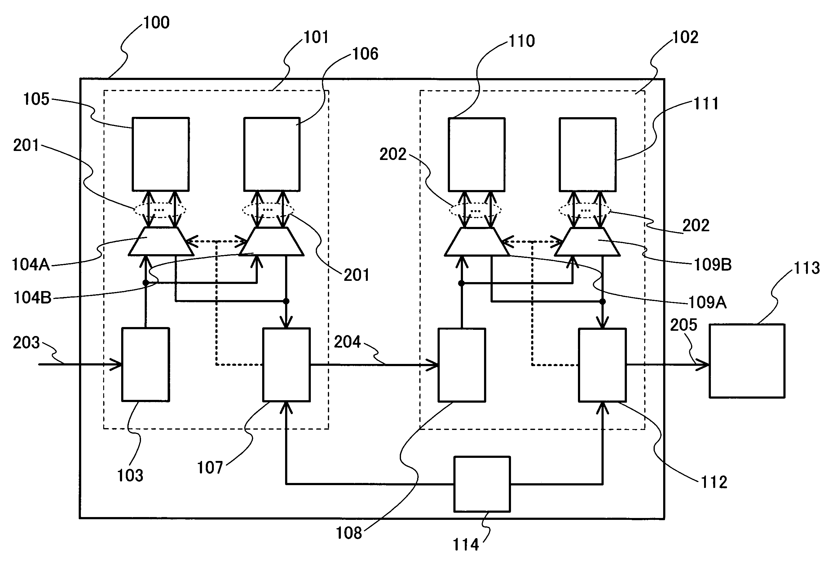
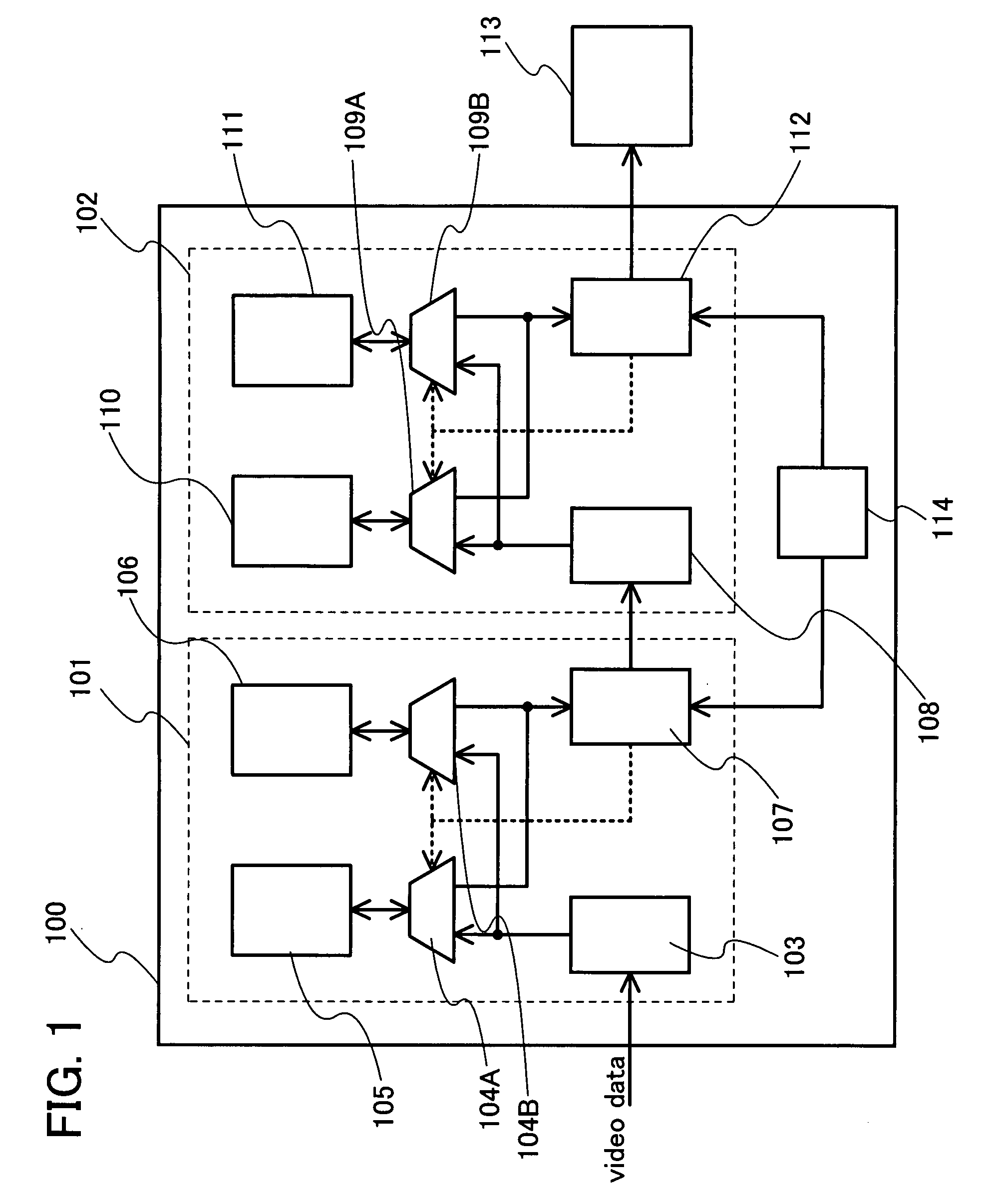
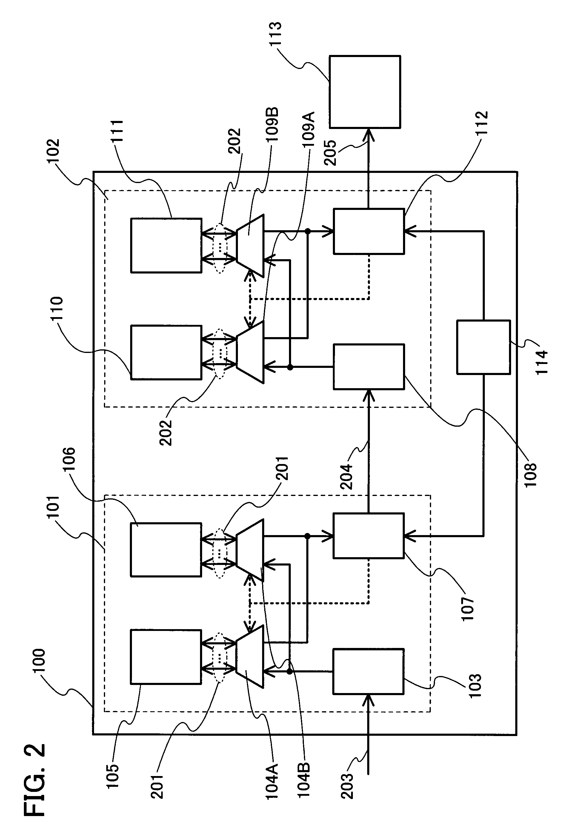
[0040]Further, in the present invention, since a pipeline processing is employed, in which a writing and reading process of video data stored in the first line memory and the second line memory, and a writing and reading process of video data stored in the first frame memory and the second frame memory are sequentially conducted, the format of the video data can be efficiently converted into the format which is actually to be displayed.

Problems solved by technology

However, since digital video data which is format-converted into a predetermined format is converted again in vertical-horizontal conversion, rearrangement of digital video data to be input to the display panel makes reading of video data stored in the frame memory complicated.
This is one reason for increase in power consumption of reading video data stored in the frame memory and for delay in access time.

Method used


Image

  • Video data control circuit, drive method thereof, and display device and electronic device having the video data control circuit
  • Video data control circuit, drive method thereof, and display device and electronic device having the video data control circuit
  • Video data control circuit, drive method thereof, and display device and electronic device having the video data control circuit

Examples


embodiment mode 1

[0062]FIG. 1 shows a block diagram of a video data control circuit in this embodiment mode. A detailed description thereof is given below. Note that, in the present invention, a video data control circuit refers to one which coverts format of inputted digital video data into a format for displaying the video data with predetermined digital gray scale, and outputs the data to a display device. In the present invention, a display device refers to a structure including a video data control circuit and a display panel provided with a plurality of pixels having a self-light emitting element such as a liquid crystal element, an EL element, or an element used in an FED. The display panel may also refer to a display panel main body which includes a plurality of pixels and a peripheral drive circuit for driving the pixels over a substrate. In addition, the display panel may also be provided with a flexible printed circuit (FPC) or a printed wiring board (PWB).

[0063]FIG. 1 illustrates a basic...

embodiment mode 2

[0093]In Embodiment Mode 2, an example of the display panel 113 in FIGS. 1 and 2 is described with reference to FIGS. 9A and 9B. In FIG. 9A, the display panel 113 has a pixel portion 901 including a plurality of pixels 900 arranged in matrix. The pixel portion 901 can have an active matrix structure in which each pixel 900 is provided with a switching element such as a thin film transistor. As a display element in the pixel 900, a light emitting element such as an electroluminescence element or the like, or a liquid crystal element may be provided. In a case where a light emitting element is provided as a display element in the pixel 900, a light emission state (bright) or a non light emission state (dark) of the pixel 900 is selected by an image signal VD.

[0094]Note that, as shown in FIG. 9B, a drive circuit which drives the pixel portion 901 may be provided over the same substrate as the pixel portion 901. In FIG. 9B, portions that are the same as those in FIG. 9A are denoted by l...

embodiment mode 3

[0096]FIG. 10A shows an example of a structure (hereinafter, referred to as a first structure) of the pixel portion 901 shown in FIGS. 9A and 9B. The pixel portion 901 includes a plurality of first signal lines S1 to Sp (p is a natural number), a plurality of second signal lines G1 to Gq (q is a natural number) which are provided so as to intersect with the plurality of first signal lines S1 to Sp, and a pixel 1000 is provided at each intersection of the first signal lines S1 to Sp and the second signal lines G1 to Gq.

[0097]A structure of the pixel 1000 in FIG. 10A is shown in FIG. 10B. FIG. 10B shows the pixel 1000 formed at an intersection of Sx (x is a natural number that is p or less) in the plurality of first signal lines S1 to Sp, and Gy (y is a natural number that is q or less) in the plurality of second signal lines G1 to Gq. The pixel 1000 includes a first transistor 1001, a second transistor 1002, a capacitor 1003, and a light emitting element 1004. Note that, in this embo...


PUM


Abstract

It is an object of the present invention to provide a video data control circuit that satisfactorily displays an image on a display panel without increasing accesses to a frame memory or increasing power consumption when conducting vertical-horizontal image display conversion when video data is converted into digital video data for displaying in a predetermined digital gray scale. Another object is to provide a display device comprising the video data control circuit in which data is temporally kept in a line memory in a video data storage portion before the data is converted into digital video data for displaying in a predetermined digital gray scale. For example, a first digital video data is written to the line memory in a first order and read from the line memory in a second order different from the first order and output to a format conversion portion as a second digital video data.

Description

BACKGROUND OF THE INVENTION[0001]1. Field of the Invention[0002]The present invention relates to a video data control circuit. In addition, the present invention relates to a drive method of a video data control circuit. Specifically, the present invention relates to a video data control circuit for controlling and holding an image signal input to a pixel in an active matrix driving display device in which each pixel is provided with a switching element. More specifically, the present invention relates to a video data control circuit for expressing gray scale by control of a period in which a pixel is in a bright state or an area in which a sub-pixel included in a pixel is in a bright state. In addition, the present invention relates to a display device including a video data control circuit of the present invention and an electronic device having the display device including the video data control circuit in a display portion.[0003]2. Description of the Related Art[0004]In recent y...

Claims


Application Information

Patent Timeline
Patent Type & Authority Applications(United States)
IPC IPC(8): G09G3/36
CPCG09G3/30G09G5/39G09G2340/0492G09G2300/0809G09G2310/0262G09G5/42G09G3/20G11C7/10
Inventor ENDO, MASAMI
Owner SEMICON ENERGY LAB CO LTD
Learn More