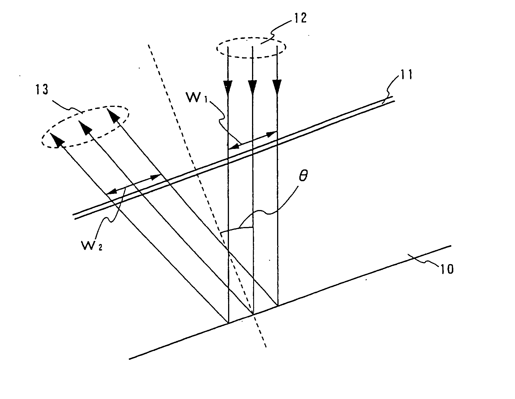
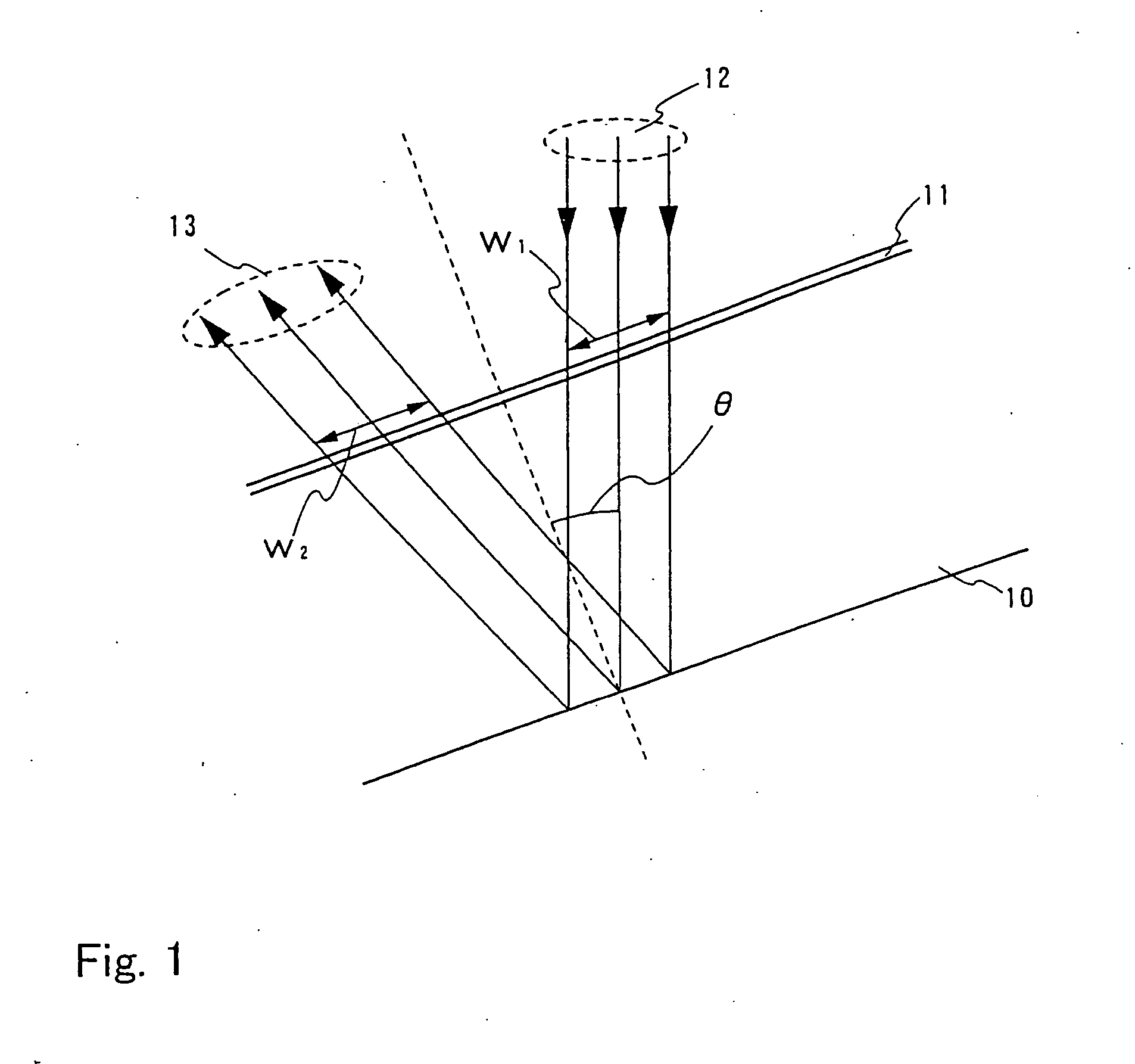
Laser annealing method and semiconductor device fabricating method
a technology of laser annealing and semiconductor devices, applied in semiconductor/solid-state device manufacturing, semiconductor devices, electrical equipment, etc., can solve problems such as interference between beams reflected, and achieve the effects of reducing the number of maintenance cycles, reducing the manufacturing cost of semiconductor devices, and low running costs
- Summary
- Abstract
- Description
- Claims
- Application Information
AI Technical Summary
Benefits of technology
Problems solved by technology
Method used
Image

Examples
embodiment 1
[0071] Embodiment 1 of the invention will be described below with reference to FIGS. 11 and 13A.
[0072] First of all, as a substrate 300, a substrate having transparency is prepared which is made of glass such as barium boro-silicate glass or alumina boro-silicate glass represented by the #7059 glass or the #1737 glass of Corning Incorporated. Incidentally, as the substrate 300, a quartz substrate or a silicon substrate may also be used. Otherwise, a plastic substrate which has heat resistance to the treatment temperature used in Embodiment 1 may also be used. In Embodiment 1, a glass substrate was prepared which was made of the #1737 glass of Corning Incorporated and was 126 mm square and 0.7 mm thick.
[0073] Then, a base film 301 made of an insulating film such as a silicon oxide film, a silicon nitride film or a silicon nitride oxide film is formed on the substrate 300. In Embodiment 1, the base film 301 may use a two-layer structure, but may also use a single-layer film made of ...
embodiment 2
[0082] Embodiment 2 which differs from Embodiment 1 will be described below with reference to FIG. 12.
[0083] A substrate and a semiconductor film were fabricated in accordance with the process of Embodiment 1. In Embodiment 2 as well, a #1737 glass substrate made by Corning Incorporated was used, and an amorphous silicon film (of thickness 55 nm) was formed over the glass substrate by a CVD method.
[0084] The optical system of Embodiment 2 will be described below with reference to FIG. 12. In FIG. 12, the same reference numerals are used to denote parts corresponding to those used in the optical system shown in FIG. 11. In Embodiment 2, the reflecting mirror 207 is fixed at 45 degrees with respect to the laser beam, and a substrate stage 203 is inclined by an angle θ from the horizontal direction.
[0085] In Embodiment 2, a YAG laser was used as the laser oscillator 201. The output from the YAG laser was modulated into the second harmonic by the non-linear optical element 202 and wa...
embodiment 3
[0086] In this embodiment, the manufacturing method of the active matrix substrate is explained using FIGS. 13 to 21.
[0087] First, in this embodiment, a substrate 300 is used, which is made of glass such as barium borosilicate glass or aluminum borosilicate, represented by such as Corning #7059 glass and #1737 glass. Note that, as the substrate 300, a quartz substrate, a silicon substrate, a metallic substrate or a stainless substrate on which is formed an insulating film. A plastic substrate with heat resistance to a process temperature of this embodiment may also be used.
[0088] Then, a base film 301 formed of an insulating film such as a silicon oxide film, a silicon nitride film or a silicon oxynitride film is formed on the substrate 300. In this embodiment, a two-layer structure is used as the base film 301. However, a single-layer film or a lamination structure consisting of two or more layers of the insulating film may be used. As a first layer of the base film 301, a silico...
PUM
 Abstract
Description
Claims
Application Information
 - R&D
- Intellectual Property
- Life Sciences
- Materials
- Tech Scout
- Unparalleled Data Quality
- Higher Quality Content
- 60% Fewer Hallucinations
Browse by: Latest US Patents, China's latest patents, Technical Efficacy Thesaurus, Application Domain, Technology Topic, Popular Technical Reports.
© 2025 PatSnap. All rights reserved.Legal|Privacy policy|Modern Slavery Act Transparency Statement|Sitemap|About US| Contact US: help@patsnap.com