
Dielectric device

a dielectric device and dielectric technology, applied in the direction of device material selection, fixed capacitor details, fixed capacitors, etc., can solve the problems of crystal properties disordered, inter-particle bond formation, cracks in the dielectric layer, etc., and achieve good yield and superior characteristics.

Inactive Publication Date: 2007-10-25
NGK INSULATORS LTD
View PDF5 Cites 13 Cited by
  • Summary
  • Abstract
  • Description
  • Claims
  • Application Information

AI Technical Summary

Benefits of technology

The present invention relates to a new type of dielectric material for use in electronic devices. This material was developed through a process called aerosol deposition, which allows for precise control over its composition and structure. By forming a smooth transition from different layers of materials, the resulting film exhibits better mechanical properties than traditional films. Additionally, the design includes a reduced gradient in stresses near the edges of the material, reducing the likelihood of crack formation during subsequent processing steps. Overall, this technology provides improved performance and reliability for electronic components utilizing high quality dielectric materials.

Problems solved by technology

Technical Problem: The technical problem addressed in this patent text relates to methods for producing different types of dielectric devices that have a reliable and efficient performance. Specifically, the focus is placed on the formation of the dielectric layers within these devices through techniques such as screen printing, green sheet method, aerosol deposition, and powder jet deposition. These methods allow for precise control over the thickness and composition of the resulting dielectric layer while also allowing for its growth at room temperature on a variety of substrates.

Method used


Image

  • Dielectric device
  • Dielectric device
  • Dielectric device

Examples


example 1

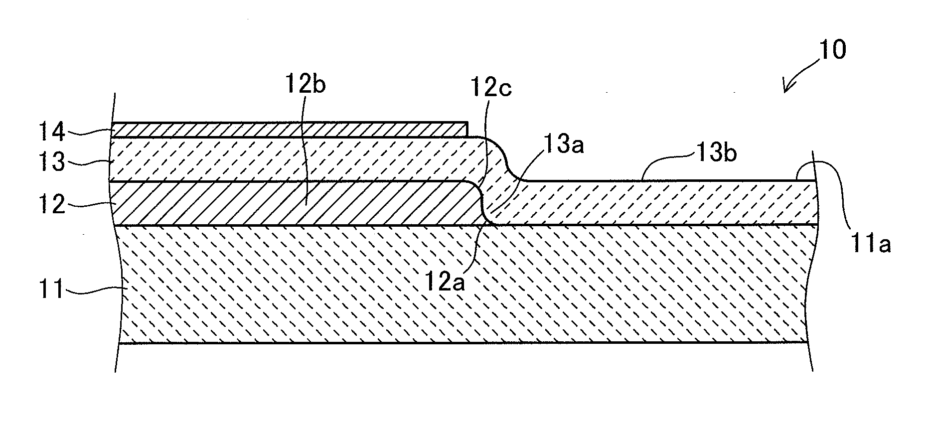
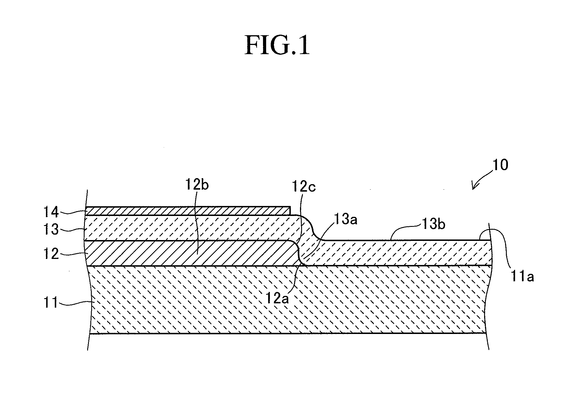
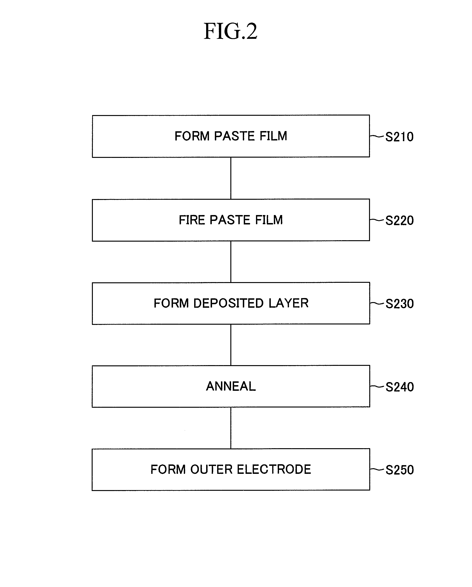
[0081]The manufacturing method of Example 1 is the manufacturing method of the first aspect shown in FIG. 2. In this first example, in the paste film-forming step S210, a film having a thickness of 4 μm of a base electrode-forming paste including a mixture of commercial silver paste and commercial glass paste is formed on the substrate surface 11a. The glass component of this glass paste is lead borosilicate glass. This base electrode-forming paste is prepared so that the ratio of glass to silver is 20% in terms of volume.

[0082]Next, in the paste film firing step S220, the aforesaid paste film is fired at 600° C. in a belt furnace.

[0083]A deposited layer of PZT formed by the aerosol deposition method, in the annealing step S240, is then annealed at 600 ° C. for 0.5 hours in a batch furnace.

[0084]The triple point adjacent part 13a in the dielectric layer 13 formed by the manufacturing method of this first example has a very fine structure as in the case of the other parts. Therefore,...

example 2

[0089]The manufacturing method of Example 2 is essentially identical to that of Example 1 except that, instead of the glass paste of Example 1, a paste of colloidal silica is used. In the base electrode-forming paste of this second example, the ratio of silica to silver is adjusted to be 20% in terms of volume.

[0090]As in the case of Example 1, the triple point adjacent part 13a in the dielectric layer 13 formed by the manufacturing method of Example 2 also has a very fine structure with no cracks.

example 3

[0091]The manufacturing method of Example 3 is essentially identical to that of Example 2 except that, instead of the silver paste of Example 1, a commercial silver resinate is used. In the base electrode-forming paste of Example 3, the ratio of silica to silver is adjusted to be 20% in terms of volume. The paste film in Example 3 is formed with a thickness of 1 μm.

[0092]As in the case of Examples 1 and 2, the triple point adjacent part 13a in the dielectric layer 13 formed by the manufacturing method of Example 3 also has a very fine structure with no cracks.


PUM

PropertyMeasurementUnit
Angleaaaaaaaaaa
Dielectric polarization enthalpyaaaaaaaaaa

Abstract

The invention suppresses the occurrence of cracks in a dielectric layer, and improve yield during manufacture of a dielectric device. A dielectric device includes a substrate, a base electrode and a dielectric layer. The base electrode is fixed on the substrate. The base electrode is formed such that a surface of a base electrode edge part has an inclined part. The dielectric layer is fixed on a substrate surface so as to cover the base electrode. The dielectric layer is formed by annealing a deposited layer obtained by spraying a powdered dielectric on the substrate surface. Therefore, a triple point adjacent part, which is a part of the dielectric layer opposite the base electrode edge part, is formed so as to have a dense structure in the same way as other parts.

Description


Claims


Application Information

Patent Timeline
Owner NGK INSULATORS LTD
Learn More