Transparent touch panel
a touch panel and transparent technology, applied in the field of transparent touch panels, can solve the problems of resistive touch devices with poor sensitivity, poor sensitivity of resistive touch screens, and the likelihood of scrap generation, and achieve the effect of reducing the optical proximity
- Summary
- Abstract
- Description
- Claims
- Application Information
AI Technical Summary
Benefits of technology
Problems solved by technology
Method used
Image

Examples
first embodiment
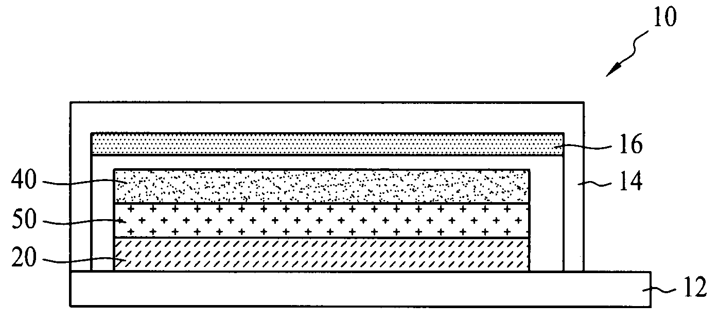
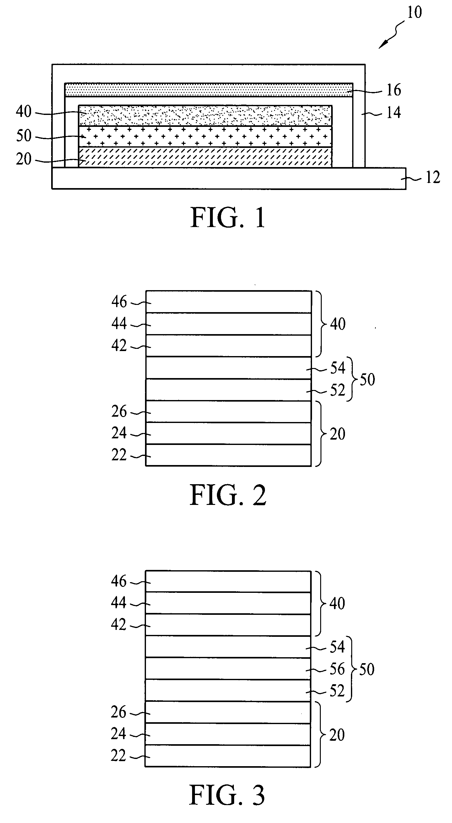
[0017]FIG. 1 to FIG. 4 illustrate a capacitive touch panel 10 according to the present invention. The capacitive touch panel 10 comprises a transparent substrate 12, a capacitive touch device 20 positioned on the transparent substrate 12, an interfacial structure 50 positioned on the capacitive touch device 20, a display device 40 positioned on the interfacial structure 50, a cap 14 adhered to the transparent substrate 12 by glue (not shown in the drawing), and an absorbent 16. The transparent substrate 12 may include transparent material such as glass, polycarbonate, polyvinyl chloride and methyl methacrylate, and the display device 40 can be an electro luminescent display device, an organic light-emitting display device, or a liquid crystal display device.
[0018]Referring to FIG. 2, the display device 40 includes an anode layer 42, a light-emitting layer 44 and a cathode layer 46. The interfacial structure 50 includes an insulating polymer layer 52 positioned on the capacitive touc...
second embodiment
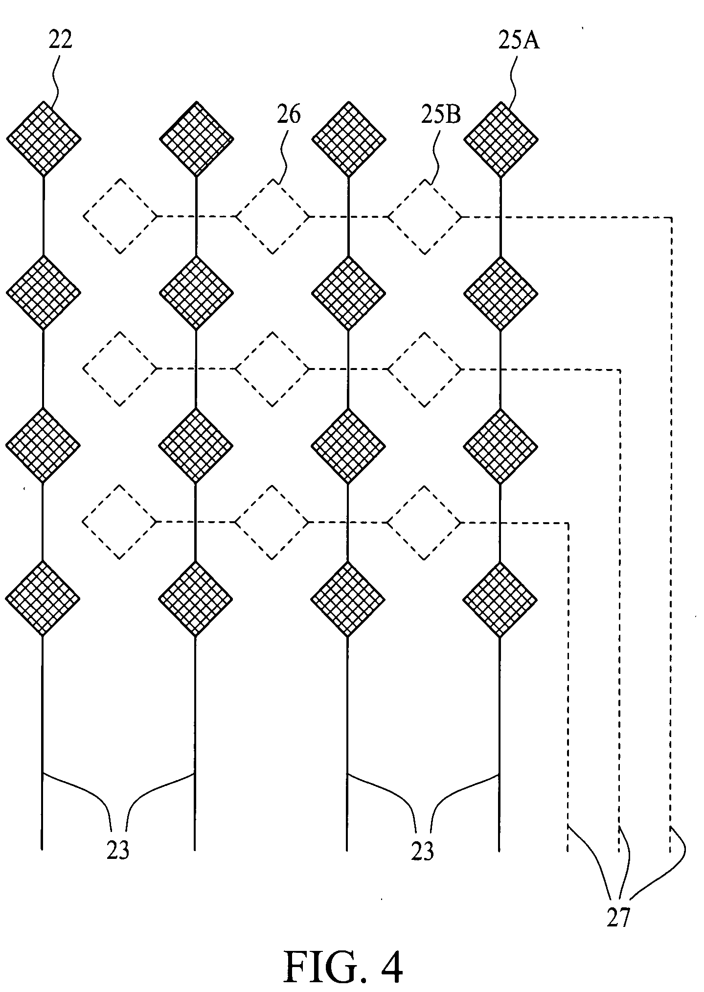
[0021]FIG. 5 illustrates a capacitive touch device 20′ according to the present invention. The capacitive touch device 20′ includes a first conductive pattern 22′ positioned on the transparent substrate 12, a plurality of first wires 23′ positioned on the transparent substrate 12, a second conductive pattern 26′ positioned on the transparent substrate 12, a dielectric layer 24′ covering the first conductive pattern 22′, the first wires 23′ and the second conductive pattern 26′, and a plurality of second wires 27′ positioned on the dielectric layer 24′. The first conductive pattern 22′ includes a plurality of first sensing blocks 25A′ positioned in an array manner, and the second conductive pattern 26′ includes a plurality of second sensing blocks 25B′ positioned in an array manner. Each first wire 23′ connects the first sensing blocks 25A′ on the same column, and each second wire 27′ connects the second sensing blocks 25B′ on the same row via a plurality of conductive plugs 28 penet...
PUM
 Abstract
Description
Claims
Application Information
 - R&D
- Intellectual Property
- Life Sciences
- Materials
- Tech Scout
- Unparalleled Data Quality
- Higher Quality Content
- 60% Fewer Hallucinations
Browse by: Latest US Patents, China's latest patents, Technical Efficacy Thesaurus, Application Domain, Technology Topic, Popular Technical Reports.
© 2025 PatSnap. All rights reserved.Legal|Privacy policy|Modern Slavery Act Transparency Statement|Sitemap|About US| Contact US: help@patsnap.com