Monitoring a monolayer deposition (MLD) system using a built-in self test (BIST) table

a monolayer deposition and monitoring system technology, applied in the field of methods, can solve problems such as affecting the ability to control and optimize processing conditions, and achieve the effect of reducing pressure in the thermal processing chamber

Inactive Publication Date: 2007-10-11
TOKYO ELECTRON LTD
View PDF11 Cites 15 Cited by
  • Summary
  • Abstract
  • Description
  • Claims
  • Application Information

AI Technical Summary

Benefits of technology

[0010] The present invention provides a method and apparatus for indicating degraded performance of the reactant flow rates in low-pressure processes. The invention provides a method of monitoring a MLD processing system that includes positioning one or more wafers in a thermal processing chamber; reducing pressure in the thermal processing chamber; performing a process on the one or more wafers; and monitoring the process using a process model, the process model being created using a set of nonlinear differential equations {dot over (x)}1 and an output equation y1, wherein

Problems solved by technology

2) In-situ measurements providing details of wafer condition, such as when saturation of a precursor monolayer is completed on the wafer(s), are not available; this hinders the ability to control and optimize processing conditions so as to achieve optimal performance and throughput.

Method used


Image

  • Monitoring a monolayer deposition (MLD) system using a built-in self test (BIST) table
  • Monitoring a monolayer deposition (MLD) system using a built-in self test (BIST) table
  • Monitoring a monolayer deposition (MLD) system using a built-in self test (BIST) table

Examples


Embodiment Construction

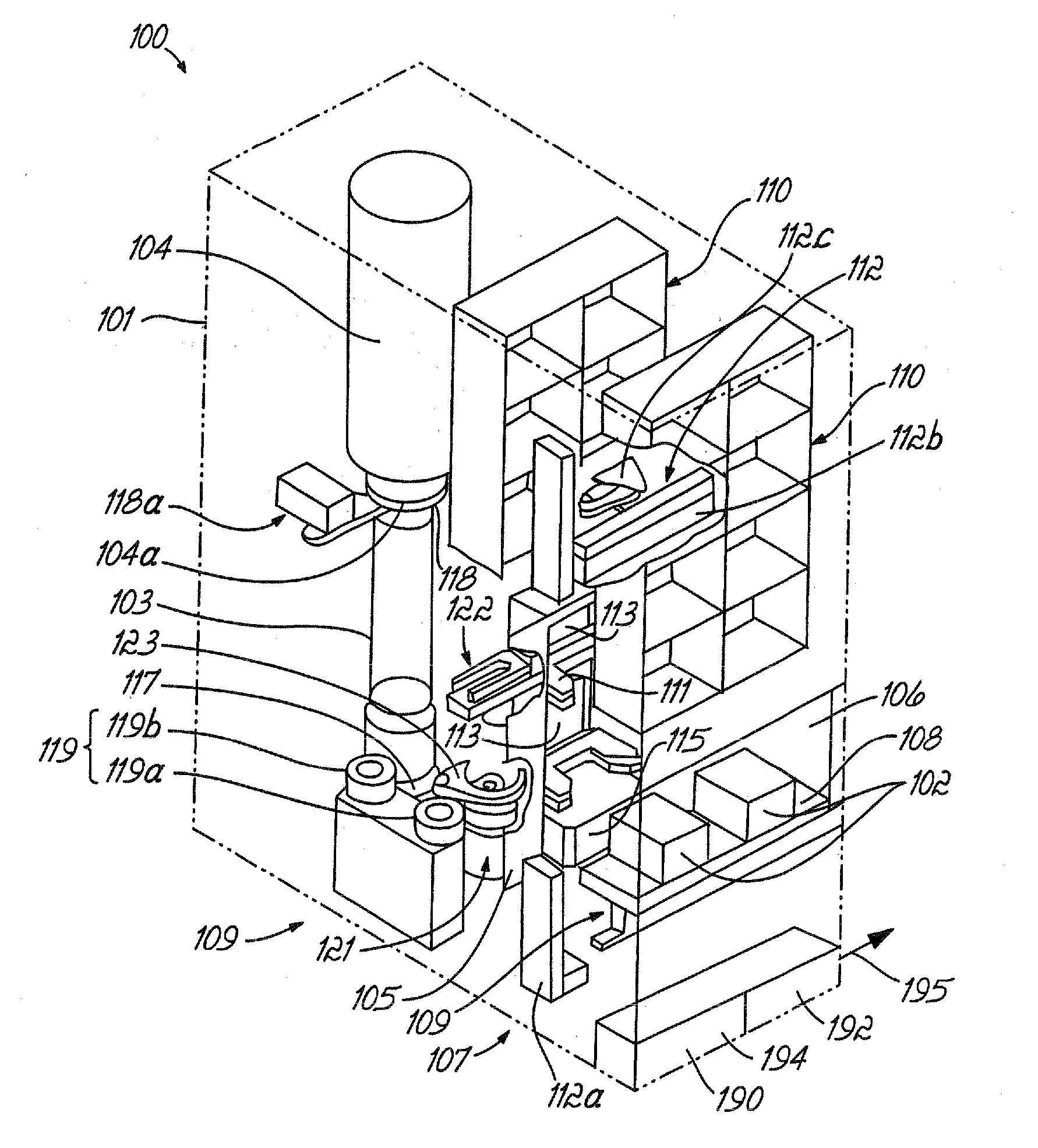
[0025] The invention relates to semiconductor manufacturing processes that involve low-pressure processing. Examples of these processes include atomic layer deposition (ALD / MLD,xLD) for films including Si3N4, Al2O3, Ta2O5, and HfSiON, chemical vapor deposition (CVD), and etch.

[0026] Such processes are conducted in both hot-wall and cold-wall processing chambers. These processing chambers are typically configured for single-wafer, multi-wafer, or batch operation. Such processing chambers can be used for processing various types of wafers, including Silicon wafers and LCD panels.

[0027] A semiconductor processing system can include a thermal processing system, an etching system, a deposition system, a plating system, a polishing system, an implant system, a developing system, or a transfer system, or a combination of two or more thereof. In addition, the process performed by the system can include a thermal process, an etching process, a deposition process, a plating process, a polis...


PUM

PropertyMeasurementUnit
diameteraaaaaaaaaa
pressureaaaaaaaaaa
pressureaaaaaaaaaa

Abstract

A method of monitoring a processing system in real-time using low-pressure based modeling techniques that include processing one or more of wafers in a processing chamber; determining a measured dynamic process response for a rate of change for a process parameter; executing a real-time dynamic model to generate a predicted dynamic process response; determining a dynamic estimation error using a difference between the predicted dynamic process response and the expected process response; and comparing the dynamic estimation error to operational limits.

Description

CROSS-REFERENCE TO RELATED APPLICATIONS [0001] This application is related to co-pending U.S. patent application Ser. No. 11 / 278,379 (Attorney Docket No. TPS-027), entitled “MONITORING A SYSTEM DURING LOW-PRESSURE PROCESSES,” filed on even date herewith; co-pending U.S. patent application Ser. No. __ / ___,___ (Attorney Docket No. TPS-031), entitled “METHOD FOR CREATING A BUILT-IN SELF TEST (BIST) TABLE FOR MONITORING A MONOLAYER DEPOSITION (MLD) SYSTEM,” filed on even date herewith, and co-pending U.S. patent application Ser. No. __ / ___,___ (Attorney Docket No. TPS-032), entitled “MONITORING A SINGLE-WAFER PROCESSING SYSTEM,” filed on even date herewith. The entire contents of these applications are herein incorporated by reference in their entirety.FIELD OF THE INVENTION [0002] This invention relates to methods for monitoring a MLD system to detect, diagnose, and predict fault conditions for a MLD system employed in low-pressure semiconductor processing. BACKGROUND OF THE INVENTION ...

Claims


Application Information

Patent Timeline
Patent Type & Authority Applications(United States)
IPC IPC(8): B05C5/00
CPCC23C16/45546C23C16/52G05B19/41875G05B23/0254G05B2219/45031G05B2219/1112G05B2219/37514G05B2219/37533G05B2219/11G05B2223/02Y02P90/02
Inventor KAUSHAL, SANJEEVPANDEY, PRADEEPSUGISHIMA, KENJI
Owner TOKYO ELECTRON LTD
Why Eureka
Try Eureka