
MIM capacitor

a capacitor and capacitor technology, applied in the direction of fixed capacitor details, fixed capacitor electrodes, electric devices, etc., can solve the problems of material with a significant permittivity being deteriorated by the subsequent component manufacturing steps, material with a significant permittivity being sometimes incompatible with the deposition conditions,

Active Publication Date: 2007-08-30
STMICROELECTRONICS (CROLLES 2) SAS
View PDF7 Cites 10 Cited by
  • Summary
  • Abstract
  • Description
  • Claims
  • Application Information

AI Technical Summary

Benefits of technology

[0016] The present invention aims at providing such a capacitor which is not an obstacle to decreasing the thickness of the interconnect metallization level in which it is formed.
[0018] The present invention aims at providing such a method which is relatively simple and inexpensive to implement in comparison with the improvements obtained in terms of the electric performance of the capacitor as well as in terms of integration surface area.

Problems solved by technology

However, the use of such materials with a significant permittivity ε raises manufacturing problems.
A problem lies in the fact that the deposition conditions of materials with a significant permittivity ε are sometimes incompatible with the presence of the components.
Another problem lies in the fact that materials with a significant permittivity ε may be deteriorated by the subsequent component manufacturing steps, in particular by the thermal cycles.
Another problem lies in the fact that it is complex to obtain a thin homogeneous layer of a material with a significant permittivity ε which is not polluted by contaminants which lower its real permittivity in an uncontrolled and variable fashion.
However, such an increase in surface area S in dielectric ILMi comes across various limits.
Especially, the increasing desire to reduce the dimensions and costs of semiconductor devices results in a decrease in the thicknesses of the metallization levels.
Further, methods of conformal deposition of thin metal layers according to complex contours are relatively difficult and expensive to implement.
In comparison with the improvements of the obtained electric performance, such solutions are considered as too expensive.
The forming of the MIM capacitors thus becomes a major obstacle to the decrease in the dimensions of the semiconductor circuits forming them.

Method used


Image

  • MIM capacitor
  • MIM capacitor
  • MIM capacitor

Examples


Embodiment Construction

[0039] For clarity, the same elements have been designated with the same reference numerals in the different drawings. Further, as usual in the representation of semiconductor circuits, the various drawings are not to scale.

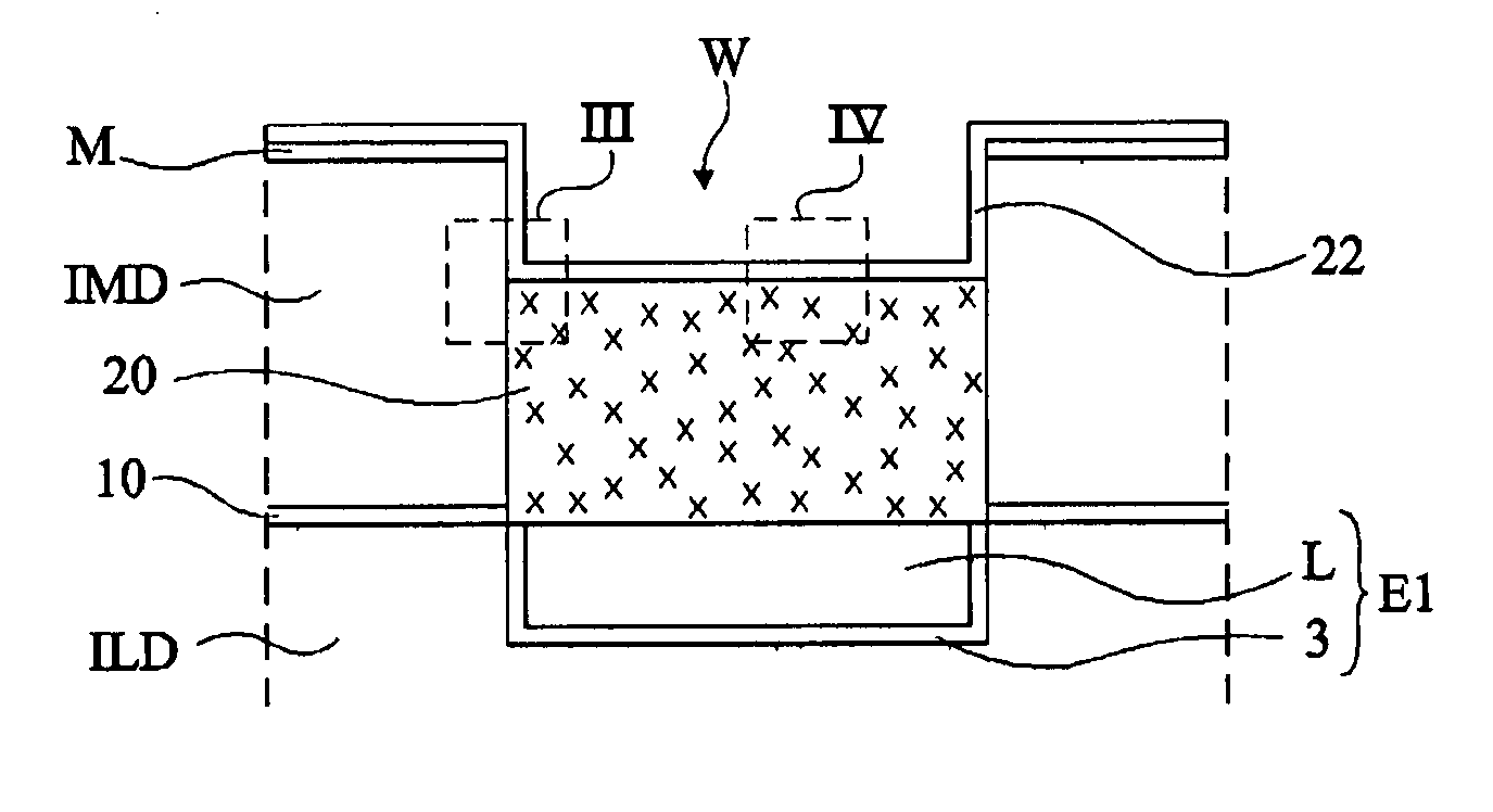
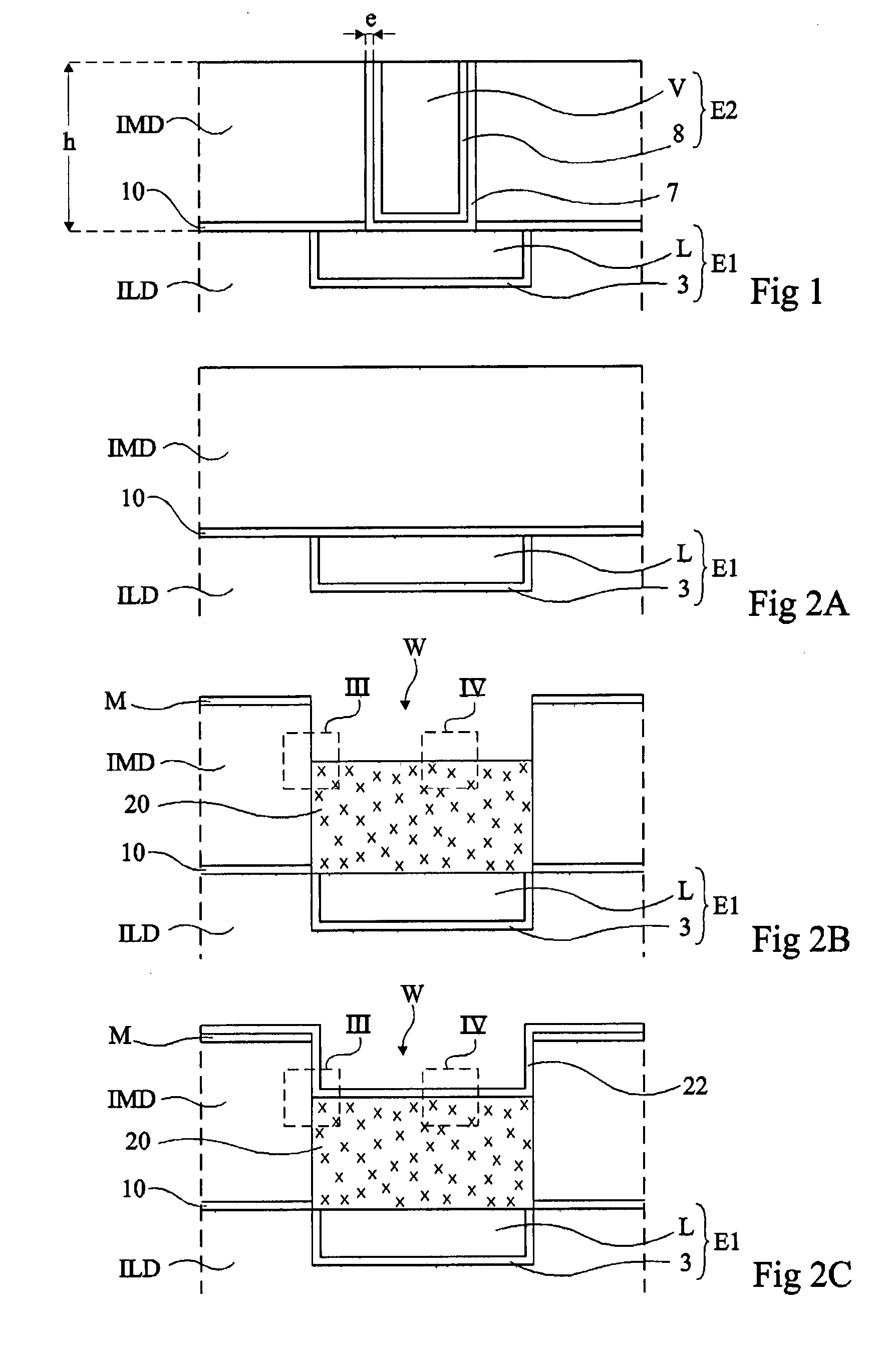
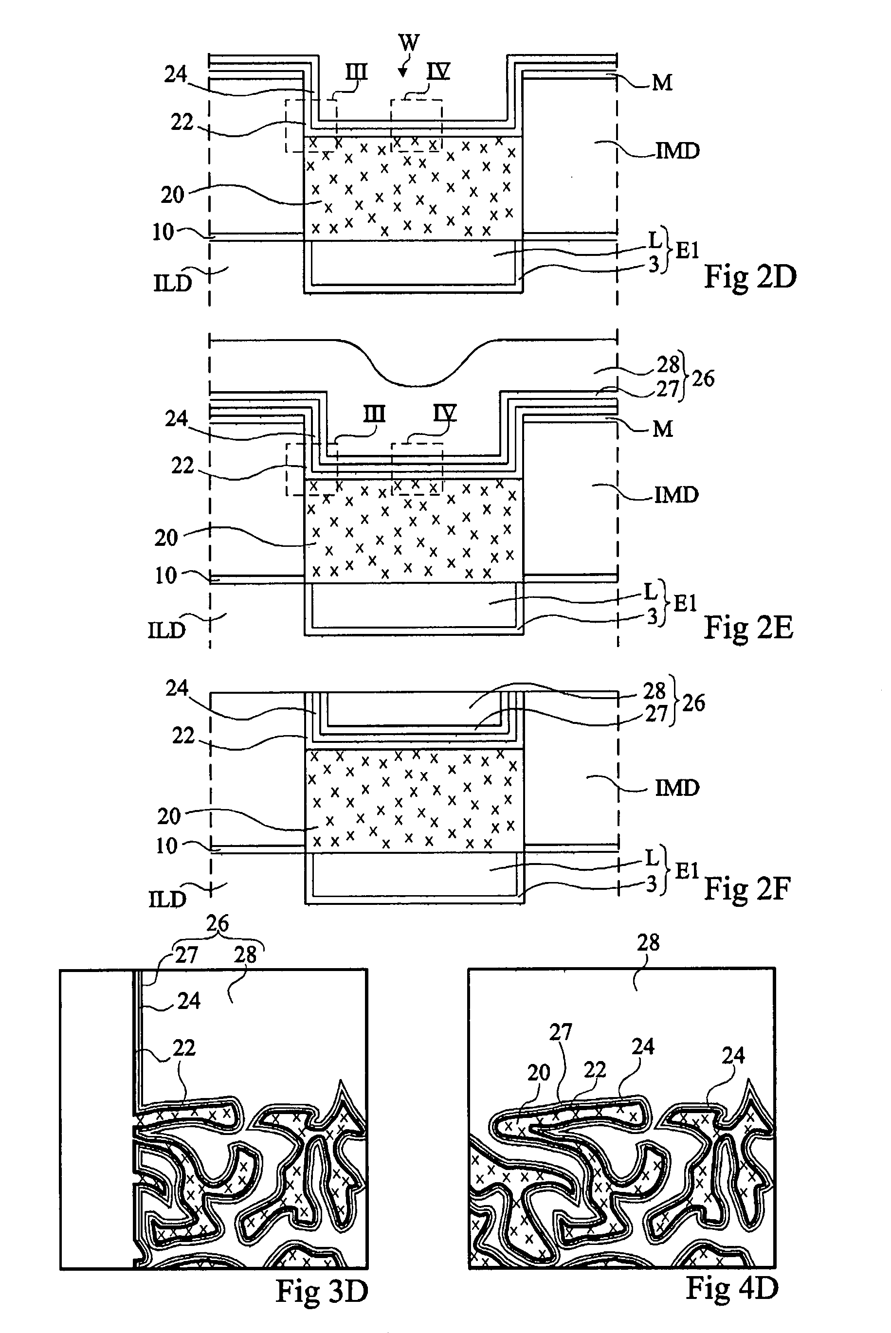
[0040]FIGS. 2A to 2E illustrate, in a cross-sectional view, different steps of the forming of a capacitor in interconnect metallization levels of a semiconductor circuit according to an embodiment of the present invention.

[0041] As illustrated in FIG. 2A, the method starts from a semiconductor circuit in which at least one interconnect metallization level is already formed. For example, a conductive line L is formed in a thick dielectric ILD. The bottom and the lateral walls of line L are preferably separated from dielectric ILD by a barrier layer 3 and a passivation layer 10 covers at least the upper surface of line L. Barrier layer 3 and passivation layer 10 are made of materials capable of avoiding the diffusion of the metal of line L. For example, line L is...


PUM


Abstract

A capacitor formed in an insulating porous material.

Description

BACKGROUND OF THE INVENTION [0001] 1. Field of the Invention [0002] The present invention relates to the manufacturing of semiconductor circuits. More specifically, the present invention relates to the structure and to the manufacturing of capacitors of metal-insulator-metal type (MIM) formed in metallization levels of interconnection of semiconductor circuits. [0003] 2. Discussion of the Related Art [0004] MIM capacitors formed in metallization levels of interconnection of semiconductor circuits are used in a great number of applications. For example, such capacitors are used as decoupling capacitors, or as filters, for example, between two circuits or components, or in voltage-controlled oscillators or else in radio-frequency applications, or else as all or part of memory elements, for example in DRAMs. . . [0005]FIG. 1 illustrates in cross-section view a known MIM capacitor. [0006] The capacitor is obtained by forming, in an interlevel dielectric ILD, a first electrode E1 of the ...

Claims


Application Information

Patent Timeline
IPC IPC(8): H01L29/00
CPCH01G4/085H01L28/84H01G4/33
Inventor TORRES, JOAQUINCHHUN, SONARITHGOSSET, LAURENT-GEORGES
Owner STMICROELECTRONICS (CROLLES 2) SAS
Learn More