Solid state imaging device and method for manufacturing the same
a technology of solid-state imaging and manufacturing methods, applied in the direction of instruments, optical elements, optical waveguide light guides, etc., can solve problems that are still unsolved, and achieve the effect of improving light sensitivity
- Summary
- Abstract
- Description
- Claims
- Application Information
AI Technical Summary
Benefits of technology
Problems solved by technology
Method used
Image
Examples
first embodiment
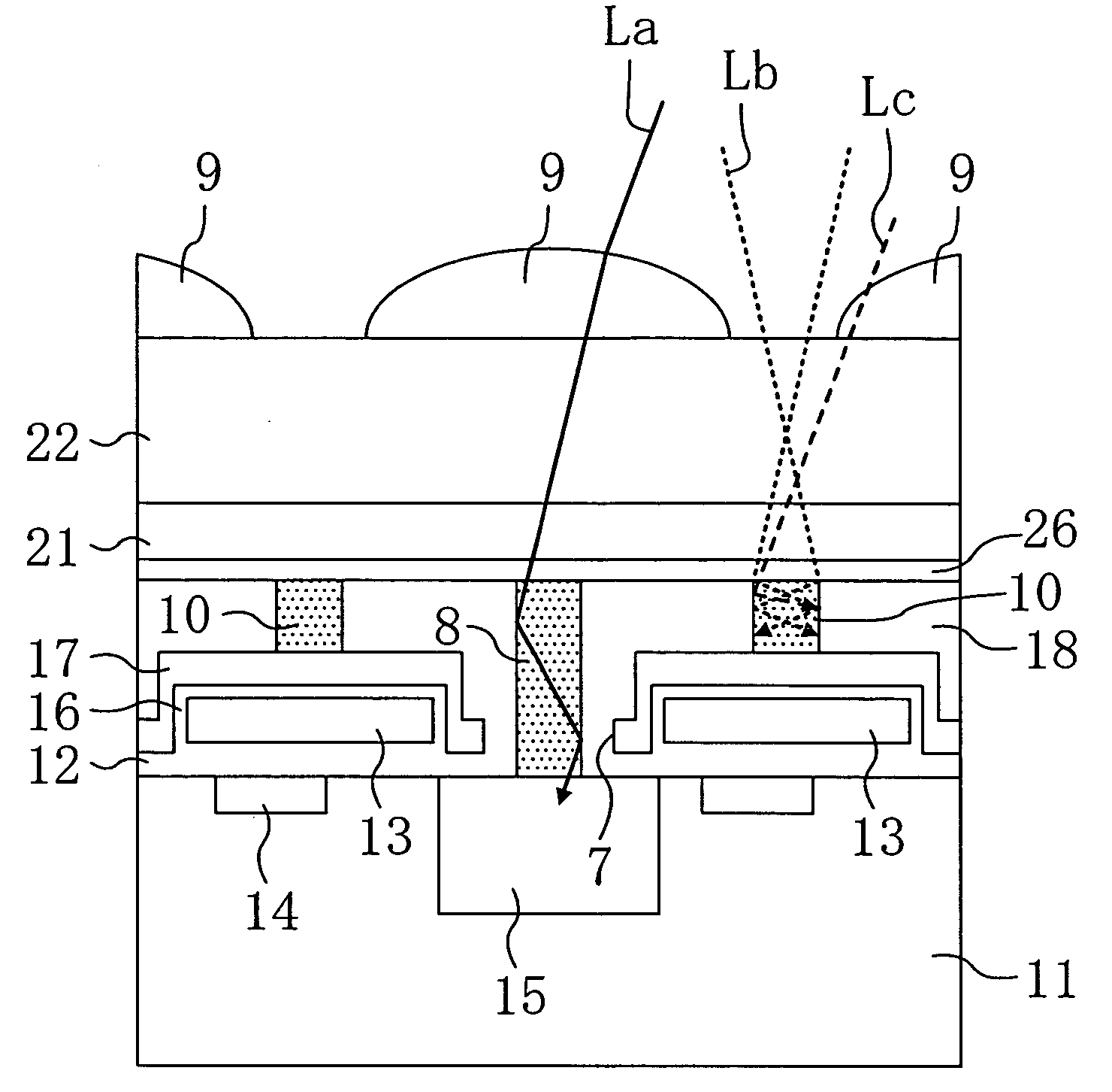
[0037]Hereinafter, explanation of a CCD solid state imaging device according to a first embodiment of the present invention is provided with reference to the drawings. As pixels in the CCD solid state imaging device of the present embodiment are provided in the same arrangement as those of the conventional device shown in FIG. 7, detailed explanation and graphic representation thereof are omitted.
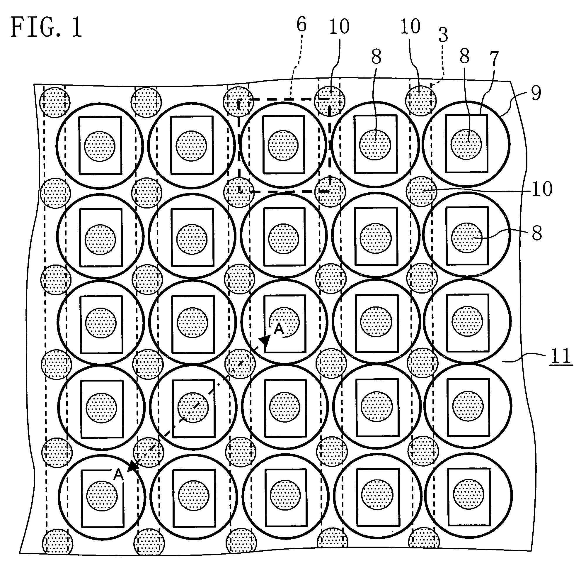
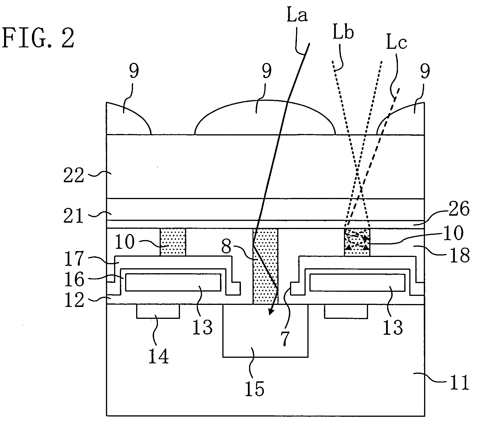
[0038]FIG. 1 is a plan view illustrating an enlargement of part of the CCD solid state imaging device according to the first embodiment and FIG. 2 is a sectional view taken along the line II-II shown in FIG. 1.
[0039]As shown in FIG. 1, the CCD solid state imaging device of the present embodiment includes a semiconductor substrate 11 on which vertical CCDs 3, openings 7 and on-chip microlenses 9 are provided. First optical waveguides 8 are formed in the openings 7 such that each of the first optical waveguides 8 is positioned at the center of the diagonal line of the opening 7. Second optica...
second embodiment
[0055]FIG. 4 is a plan view illustrating an enlargement of part of a CCD solid state imaging device according to a second embodiment. In the solid state imaging device of the present embodiment, light absorbers 25 are provided below the second optical waveguides 10, i.e., between the second optical waveguides 10 and the light shield film 17. This structure makes it possible to reduce re-reflection of light to a further extent. Other structures and effects of the present embodiment are the same as those of the first embodiment and therefore the explanation is omitted.
Other Embodiments
[0056]In the first and second embodiments described above, explanation is made with the CCD solid state imaging device taken as an example. However, the solid state imaging device of the present invention may be a MOS solid state imaging device.
[0057]In the first and second embodiments described above, the second optical waveguides 10 are round-shaped when viewed in plan (FIG. 1). However, the planar sha...
PUM
 Abstract
Description
Claims
Application Information
 - R&D
- Intellectual Property
- Life Sciences
- Materials
- Tech Scout
- Unparalleled Data Quality
- Higher Quality Content
- 60% Fewer Hallucinations
Browse by: Latest US Patents, China's latest patents, Technical Efficacy Thesaurus, Application Domain, Technology Topic, Popular Technical Reports.
© 2025 PatSnap. All rights reserved.Legal|Privacy policy|Modern Slavery Act Transparency Statement|Sitemap|About US| Contact US: help@patsnap.com


