
Semiconductor device having alignment post electrode and method of manufacturing the same

a technology of semiconductor devices and post electrodes, which is applied in the direction of semiconductor devices, semiconductor/solid-state device details, electrical apparatus, etc., can solve the problems of large error rate, inability to maintain alignment accuracy, and high recognition error rate, so as to efficiently execute alignment and reliably recognize alignment marks

Active Publication Date: 2007-07-19
AOI ELECTRONICS CO LTD
View PDF10 Cites 32 Cited by
  • Summary
  • Abstract
  • Description
  • Claims
  • Application Information

AI Technical Summary

Benefits of technology

[0011] It is an object of the present invention to provide a semiconductor device and a method of manufacturing the same, which can reliably recognize an alignment mark and efficiently execute alignment after post electrode formation.

Problems solved by technology

Conventionally, if a photomask is aligned by using the orientation flat of a semiconductor integrated circuit wafer, in order to forming post electrodes for external connection on connection pads formed on the wafer, the error becomes large.
However, when the number of post electrodes increases, and / or the array pitch between them decreases, the alignment accuracy cannot be maintained even on the basis of the opening portions of the insulating film.
In this case, it is difficult to identify post electrodes serving as alignment marks and the remaining post electrodes, resulting in high recognition error rate.

Method used


Image

  • Semiconductor device having alignment post electrode and method of manufacturing the same
  • Semiconductor device having alignment post electrode and method of manufacturing the same
  • Semiconductor device having alignment post electrode and method of manufacturing the same

Examples


first embodiment

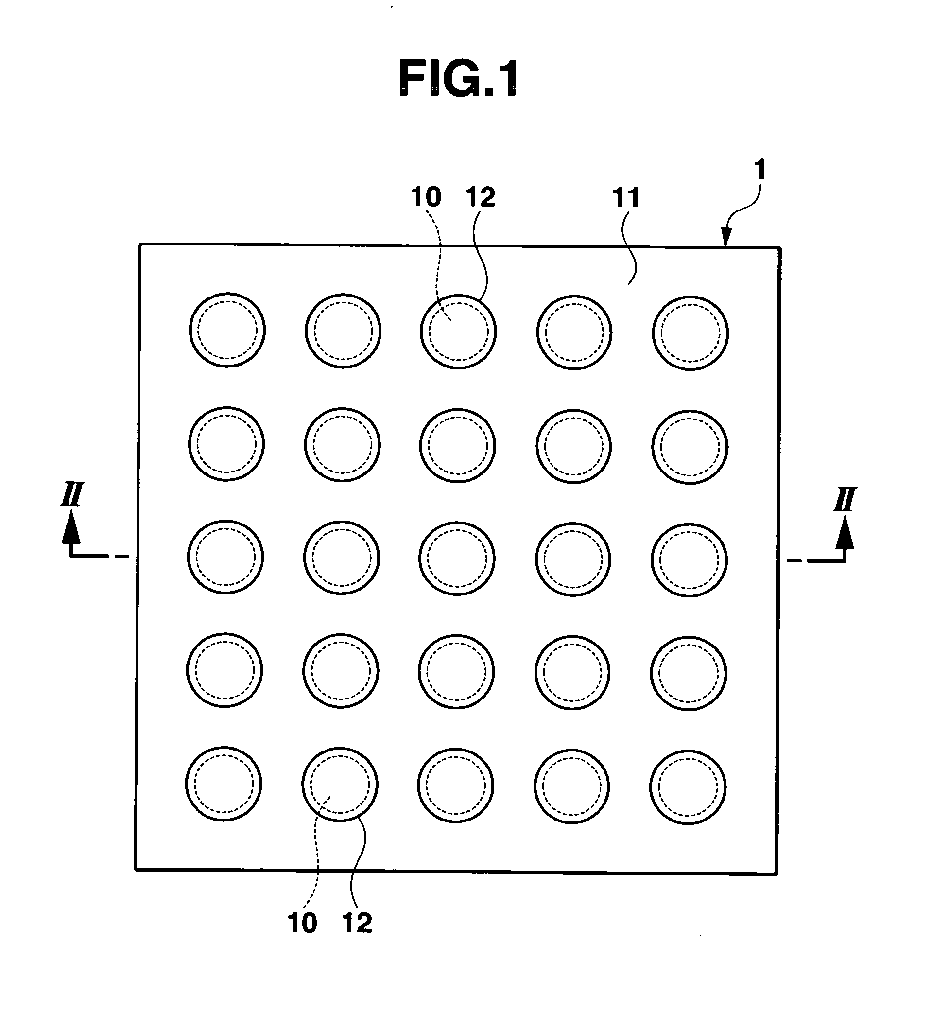
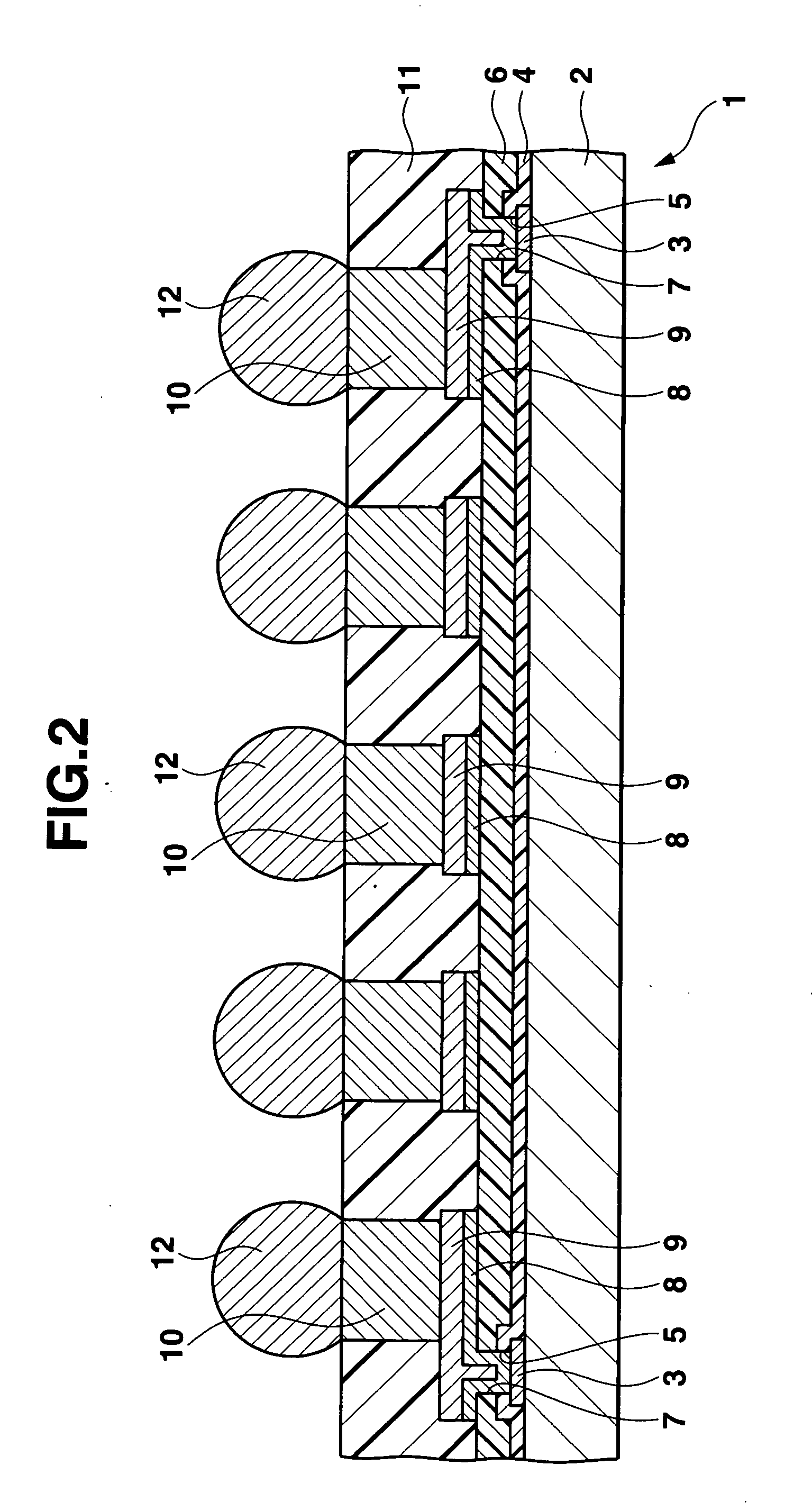
[0094]FIG. 1 is a plan view of a semiconductor element 1 of a semiconductor device according to an embodiment of the present invention. FIG. 2 is a sectional view taken along a line II-II in FIG. 1. The semiconductor element 1 is called a CSP (Chip Size Package) and has a silicon substrate 2 having a square planar shape. An integrated circuit (not shown) is formed at the central portion of the upper surface of the silicon substrate 2. A plurality of connection pads 3 made of, e.g., an aluminum-based metal are formed at the peripheral portion of the upper surface and electrically connected to the integrated circuit.

[0095] An insulating film 4 made of silicon oxide or silicon nitride and a protective film 6 made of polyimide are sequentially formed on the upper surface of the silicon substrate 2 except the central portion of each connection pad 3. The central portion of each connection pad 3 is exposed through an opening portion 5 formed in the insulating film 4 and an opening portio...

second embodiment

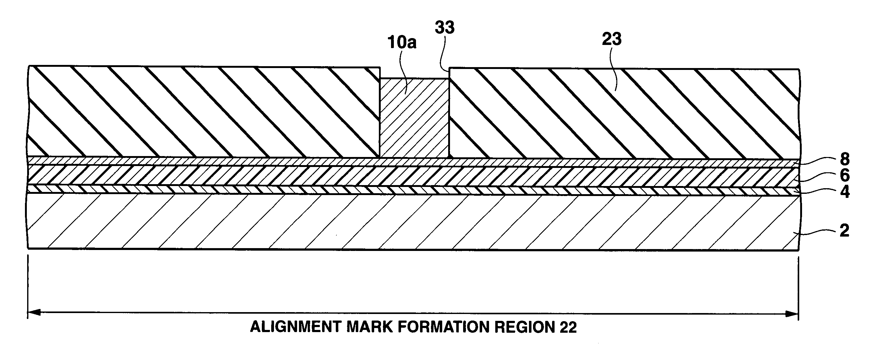
[0116] For example, as in the second embodiment of the present invention shown in FIG. 20, regions marked with ◯ around alignment mark formation regions 22 may be non-semiconductor device formation regions 41 each having the same planar size as a semiconductor device formation region 21 and having no post electrode. In this case, since the non-semiconductor device formation regions 41 having no post electrode exist between the alignment mark formation regions 22 and semiconductor device formation regions 21, any alignment mark recognition error can more reliably be prevented.

[0117] A method of forming the non-semiconductor device formation regions 41 shown in FIG. 20 will be described next. In this case, a third exposure mask 42 shown in FIG. 21 is prepared in advance in addition to first exposure mask 24 and second exposure mask 25. In the third exposure mask 42, a square glass plate 43 has a transparent portion 44 in an entire predetermined region corresponding to the non-semicon...

third embodiment

[0123]FIG. 26 is a sectional view taken along a line II-II in FIG. 1. A semiconductor element 1 is called a CSP (Chip Size Package) and has a silicon substrate 2 having a square planar shape. A semiconductor integrated circuit (not shown) having a predetermined function is formed at the central portion of the upper surface of the silicon substrate 2. A plurality of connection pads 3 made of, e.g., an aluminum-based metal are formed at the peripheral portion of the upper surface and connected to the semiconductor integrated circuit.

[0124] An insulating film 4 made of silicon oxide or silicon nitride is formed on the upper surface of the silicon substrate 2 except the central portion of each connection pad 3. The central portion of each connection pad 3 is exposed through an opening portion 5 formed in the insulating film 4. A protective film (insulating film) 6 made of epoxy resin or polyimide resin is formed on the upper surface of the insulating film 4. In this case, an opening po...


PUM


Abstract

A semiconductor device includes a semiconductor substrate which has a plurality of semiconductor device formation regions and alignment mark formation region having the same planar size as that of the semiconductor device formation region, a plurality of post electrodes which are formed in each semiconductor device formation region, and an alignment post electrode which is formed in the alignment mark formation region and smaller in number than the post electrodes formed in each semiconductor device formation region.

Description

CROSS-REFERENCE TO RELATED APPLICATIONS [0001] This is a Continuation-in-Part application of U.S. patent application Ser. No. 10 / 853,728, filed May 24, 2004, now abandoned, the entire contents of which are incorporated herein by reference. [0002] This application is based upon and claims the benefit of priority from prior Japanese Patent Applications No. 2003-147448, filed May 26, 2003; No. 2003-320581, filed Sep. 12, 2003; and No. 2006-039135, filed Feb. 16, 2006, the entire contents of all of which are incorporated herein by reference.BACKGROUND OF THE INVENTION [0003] 1. Field of the Invention [0004] The present invention relates to a semiconductor device having an alignment post electrode and a method of manufacturing the same. [0005] 2. Description of the Related Art [0006] Conventionally, if a photomask is aligned by using the orientation flat of a semiconductor integrated circuit wafer, in order to forming post electrodes for external connection on connection pads formed on t...

Claims


Application Information

Patent Timeline
IPC IPC(8): H01L23/48H01L21/44
CPCH01L23/3114H01L23/544H01L24/13H01L24/11H01L2924/014H01L2223/54453H01L2223/54466H01L2223/5448H01L2224/1147H01L2224/13099H01L2224/16H01L2924/01013H01L2924/01022H01L2924/01029H01L2924/01075H01L2924/01078H01L2924/14H01L2924/3025H01L2924/01033H01L2924/00H01L2224/11H01L2224/13H01L2224/05024H01L2224/05008H01L2224/05022H01L2224/05548H01L2224/05001H01L2224/05124H01L2224/05147H01L2224/05647H01L2224/05166H01L24/05H01L24/03H01L2224/02377H01L2224/05569H01L2224/06131H01L2924/00014
Inventor WAKISAKA, SHINJIITO, TOMOHIROYOKOYAMA, SHIGERUKUWABARA, OSAMUKANEKO, NORIHIKOKOTANI, SYOUICHI
Owner AOI ELECTRONICS CO LTD
Learn More