


Quick Research
Generate reliable direction feasibility study reports for your R&D in just a few steps.

Technical Q&A
Discover and master advanced knowledge NOW. Basics, ideas, possibilities, all at once.

Find Solutions
As an expert in R&D theories, this can generate solutions to your technical problems instantly.

Evaluate Feasibility
Analyze your overall solution with one click, know your potential R&D risks in advance.

Monitor Landscape
Get weekly tech updates, stay abreast of the latest tech innovations and key insights.
Conductor contacts with enhanced reliability
a technology of reliability and conductors, applied in the field of conductor contacts, can solve the problems of resistive loss and loss factors, and achieve the effect of facilitating the exposing of the conductor contact region
- Summary
- Abstract
- Description
- Claims
- Application Information
AI Technical Summary
Benefits of technology
Problems solved by technology
Method used
Image


Examples
first embodiment
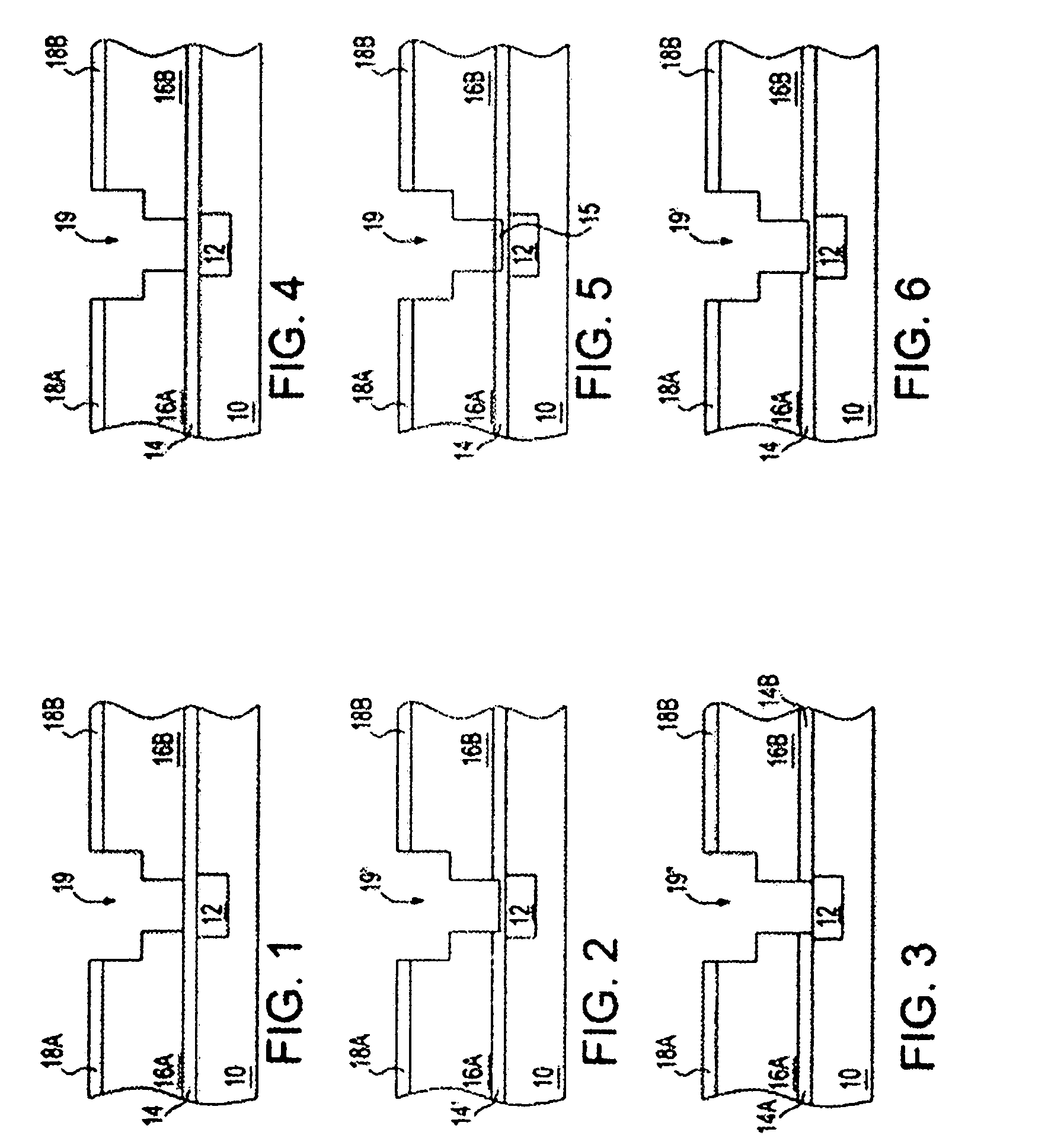
[0026]FIG. 1 to FIG. 3 show a series of schematic cross-sectional diagrams illustrating the results of progressive initial processing of a conductor contact structure in accordance with the invention.
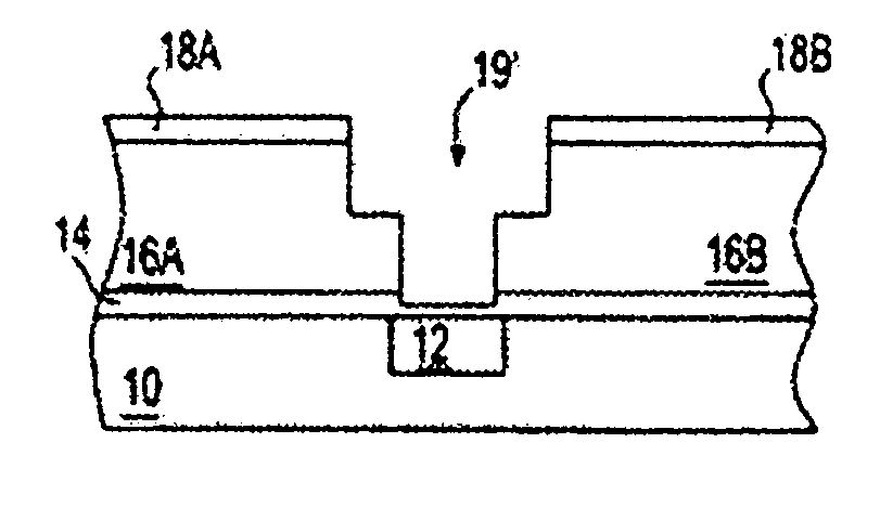
[0027]FIG. 1 shows a substrate 10 having a conductor contact region 12 located therein. A blanket capping layer 14 is located upon the substrate 10 including the conductor contact region 12. A pair of patterned inter-level dielectric layers 16a and 16b is located upon the blanket capping layer 14. Finally, a pair of patterned hard mask layers 18a and 18b is located aligned upon the pair of patterned inter-level dielectric layers 16a and 16b. The pair of patterned inter-level dielectric layers 16a and 16b, and the pair of patterned hard mask layers 18a and 18b, define a dual damascene aperture 19 that exposes a portion of the blanket capping layer 14 that is located upon the conductor contact region 12.
[0028] The substrate 10 and each of the foregoing layers located thereupon or thereov...
second embodiment
[0051]FIG. 4 to FIG. 7 show a series of schematic cross-sectional diagrams illustrating the invention that also etches the blanket capping layer 14 to expose the conductor contact region 12 located thereunder.
[0052] In a first instance, FIG. 4 shows a schematic cross-sectional diagram of a microelectronic structure analogous, equivalent or identical to the microelectronic structure whose schematic cross-sectional diagram is illustrated in FIG. 1. Like or identical components are designated with identical reference numerals.
[0053]FIG. 5 shows the results of partially converting (rather than partially etching) an upper thickness of the blanket capping layer 14 over the conductor contact region 12 to also form the thinned blanket capping layer 14′. In comparison with FIG. 2, however, a converted material layer 15 is located upon the thinned blanket capping layer 14′ over the conductor contact region 12.
[0054] Within the second embodiment as illustrated in FIG. 5, the converted materi...
third embodiment
[0063]FIG. 8 to FIG. 10 show a series of schematic cross-sectional diagrams illustrating the results of progressive stages in fabricating a conductor contact structure in accordance with the invention.
[0064]FIG. 8 is analogous, equivalent or identical to FIG. 4 or FIG. 1, and again identical reference numerals are used for like or identical structures.
[0065] As illustrated in FIG. 9, the third embodiment contemplates that the blanket capping layer 14 as illustrated in FIG. 8 is completely converted at the base of the dual damascene aperture 19 to provide a converted material layer 15′, as well as the pair of patterned capping layers 14a and 14b. The converted material layer 15′ is converted for its entire thickness and it reaches the conductor contact region 12.
[0066]FIG. 10 shows the results of stripping the converted material layer 15′ to expose the conductor contact region 12. The converted material layer 15′ as illustrated in FIG. 9 may be stripped using methods and materials ...
PUM
| Property | Measurement | Unit |
|---|---|---|
| Thickness | aaaaa | aaaaa |
| Electrical conductor | aaaaa | aaaaa |
| Exposure limit | aaaaa | aaaaa |
Abstract
Description
Claims
Application Information
 - R&D Engineer
- R&D Manager
- IP Professional
- Industry Leading Data Capabilities
- Powerful AI technology
- Patent DNA Extraction
Browse by: Latest US Patents, China's latest patents, Technical Efficacy Thesaurus, Application Domain, Technology Topic, Popular Technical Reports.
© 2024 PatSnap. All rights reserved.Legal|Privacy policy|Modern Slavery Act Transparency Statement|Sitemap|About US| Contact US: help@patsnap.com