Method for fabricating reverse-staggered thin film transistor

a polycrystalline silicon and transistor technology, applied in the field of reversestaggered polycrystalline silicon thin film transistors, can solve the problems of difficult to ensure a uniform crystallization of samples, requires expensive laser equipment, and requires a long heating time, so as to reduce metal contamination and uniform grain size of polycrystalline materials.

Inactive Publication Date: 2007-06-14
UNIV IND COOP GRP OF KYUNG HEE UNIV
View PDF2 Cites 12 Cited by
  • Summary
  • Abstract
  • Description
  • Claims
  • Application Information

AI Technical Summary

Benefits of technology

[0012] In an attempt to solve the above-mentioned problems of the prior arts, it is an object of the present invention to provide a method for fabricating a reverse-staggered polycrystalline silicon thin film transistor that reduces a metal contamination and realizes gate planarization by a gate insulating film of phosphosilicate-spin-on-glass (P-SOG) absorbing metal residues left on a polycrystalline silicon thin film formed on accordance with crystallization of an amorphous silicon thin film, and achieves a uniform grain size of the polycrystalline silicon thin film by a cap layer formed on the amorphous silicon thin film, thereby ensuring a clean and flat surface.

Problems solved by technology

However, the laser beam radiation makes it difficult to ensure a uniform crystallization of a sample when the sample has a large area, and requires expensive laser equipment.
However, the solid phase crystallization requires a high crystallization temperature and a long heating time.
Furthermore, polycrystalline silicon grains formed by the solid phase crystallization may have many defects, thereby making it difficult to fabricate devices using the polycrystalline silicon thin film.
In addition, due to the high crystallization temperature, it is impossible to use a glass substrate.
However, the polycrystalline silicon thin film fabricated by this crystallization may have defects in device structure resulting from a metal contamination, thereby having a limitation on electric properties.
However, there has been no technology capable of completely solving a metal contamination, which is a primary problem of the polycrystalline silicon thin film.

Method used


Image

  • Method for fabricating reverse-staggered thin film transistor
  • Method for fabricating reverse-staggered thin film transistor
  • Method for fabricating reverse-staggered thin film transistor

Examples


Embodiment Construction

[0040] Hereinafter, reference will now be made in detail to the preferred embodiments of the present invention associated with a method fabricating a reverse-staggered polycrystalline silicon thin film transistor according to the present invention, examples of which are illustrated in the annexed drawings.

[0041]FIG. 1 is a flow chart illustrating a method for fabricating a reverse-staggered polycrystalline silicon thin film transistor according to an embodiment of the present invention.

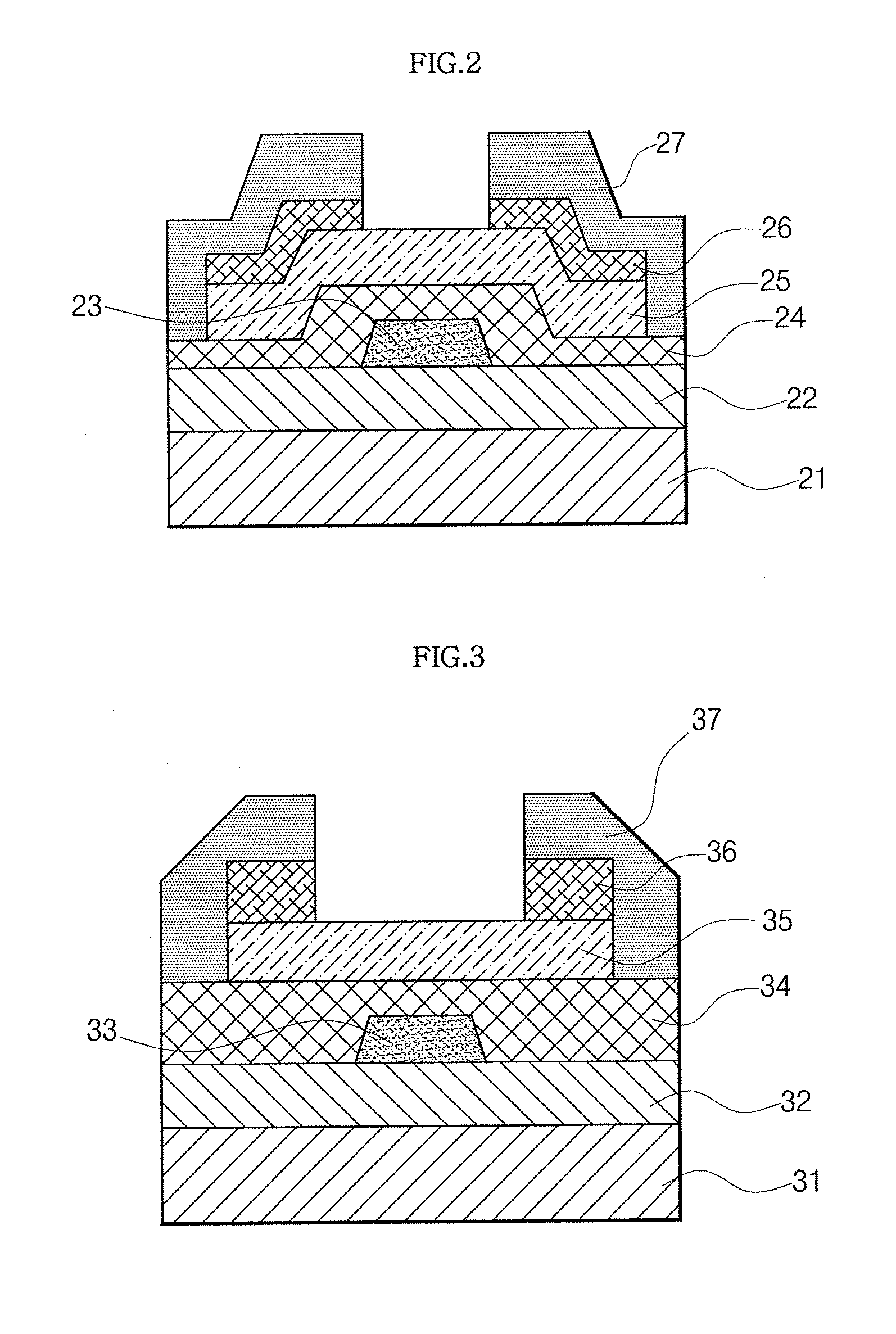
[0042] As shown in FIG. 1, the method fabricating a reverse-staggered polycrystalline silicon thin film transistor comprises the steps of: forming a buffer layer on an insulating substrate (S10); forming a gate metal pattern on the buffer layer (S20); forming a planarized gate insulating film on the gate metal pattern (S30); depositing an amorphous silicon layer on the gate insulating film (S40); crystallizing the amorphous silicon layer into a polycrystalline silicon layer (S50); forming an n+ or p...


PUM

PropertyMeasurementUnit
thicknessaaaaaaaaaa
grain sizeaaaaaaaaaa

Abstract

Disclosed herein is a method for fabricating a reverse-staggered polycrystalline silicon thin film transistor, and more specifically a method for fabricating a reverse-staggered polycrystalline silicon thin film transistor wherein a phosphosilicate-spin-on-glass (P-SOG) is used for a gate insulating film. The method comprises the steps of: forming a buffer layer on an insulating substrate; forming a gate metal pattern on the buffer layer; forming a planarized gate insulating film on the gate metal pattern; depositing an amorphous silicon layer on the gate insulating film; crystallizing the amorphous silicon layer into a polycrystalline silicon layer; forming a n+ or p+ layer on the polycrystalline silicon layer; forming a source / drain metal layer on the n+ or p+ layer; and forming a passivation layer on the source / drain metal layer.

Description

BACKGROUND OF THE INVENTION [0001] 1. Field of the Invention [0002] The present invention relates to a method for fabricating a reverse-staggered polycrystalline silicon thin film transistor, and more specifically to a method for fabricating a reverse-staggered polycrystalline silicon thin film transistor wherein a phosphosilicate-spin-on-glass (P-SOG) is used for a gate insulating film. [0003] 2. Description of the Related Art [0004] Devices using a polycrystalline silicon thin film are mainly utilized in a variety of appliances including active devices of active matrix liquid crystal displays (AMLCDs), and switching devices and peripheral circuits of electroluminescent (EL) devices. [0005] Since the devices using the polycrystalline silicon thin film are suitable for realization in a high response rate and a large pixel number, they can greatly contribute to obtaining a superior picture quality, large-size screen and excellent color representation of display devices. [0006] Laser ...

Claims


Application Information

Patent Timeline
Patent Type & Authority Applications(United States)
IPC IPC(8): H01L21/84
CPCH01L29/04H01L27/1296H01L29/78678H01L29/66765H01L21/02672H01L29/4908
Inventor JANG, JINCHEON, JUN-HYUK
Owner UNIV IND COOP GRP OF KYUNG HEE UNIV
Why Eureka
Try Eureka