Method for fabricating thin layer device

Inactive Publication Date: 2007-06-07
NAT INST OF INFORMATION & COMM TECH
View PDF5 Cites 6 Cited by
  • Summary
  • Abstract
  • Description
  • Claims
  • Application Information

AI Technical Summary

Benefits of technology

[0011] Subsequently, it is an object of the present invention to provide a method for producing a thin layer device excellent in mechanical strength and ensuring sufficient thickness, by mounting an epitaxial multilayer structure substance such as an NbN / MgO / NbN-SIS junction on a SiO2 substrate which is useful as material for a submillimeter band.
[0013] The present inventors have extensively studied on production technology of an NbN / MgO / NbN-SIS junction to solve the above-described problems and found that by using MgO as a temporary substrate, and producing an epitaxial NbN / MgO / NbN-SIS junction composed of an NbN layer / an MgO layer / an NbN layer formed by epitaxial growth (hereinafter called also as an epitaxial NbN / MgO / NbN) on the temporary substrate, and by subsequent film forming of SiO2 having a thickness of several tens μm as a substrate on the NbN / MgO / NbN-SIS junction produced by epitaxial growth, and then by removing the above MgO temporary substrate by an acid and the like, a thin layer device mounted with the NbN / MgO / NbN-SIS junction on a SiO2 substrate having a thickness of several tens μm can be produced, and also found that by using the above thin layer device mounted with the NbN / MgO / NbN-SIS junction on a SiO2 substrate which has particularly excellent mechanical strength and is effective as material for a submillimeter band, a superconductive device, a mixer, and an HEB electromagnetic wave receiver composed of the thin layer device can be obtained, and have thus completed the present invention.
[0014] According to the present invention, uniformly polishing technology is not required, because SiO2 having a thickness of several tens μm is formed as a substrate by a film forming method, and the above MgO temporary substrate is removed by etching, and moreover, sufficient substrate thickness can be secured and a superconductive device in mechanical strength can be produced, compared with using MgO as a substrate, because SiO2 having relatively low dielectric constant is used as a substrate. In addition, excellent control of substrate thickness is possible because a substrate of SiO2 and the like is produced by a film forming method.
[0015] The above thin layer device includes a superconductive device such as an SIS receiver or an HEB receiver. Production of a grounding conductor is also possible by film forming and lithography during production of a thin film device, which enables to attain steady and good grounding.

Problems solved by technology

However, an MgO single crystal substrate is labile to crack by cleavage and the like, and a thin substrate causes mechanical strength reduction, which make substantially difficult to obtain arbitrary substrate thickness in good reproducibility.

Method used


Image

  • Method for fabricating thin layer device
  • Method for fabricating thin layer device
  • Method for fabricating thin layer device

Examples


example 1

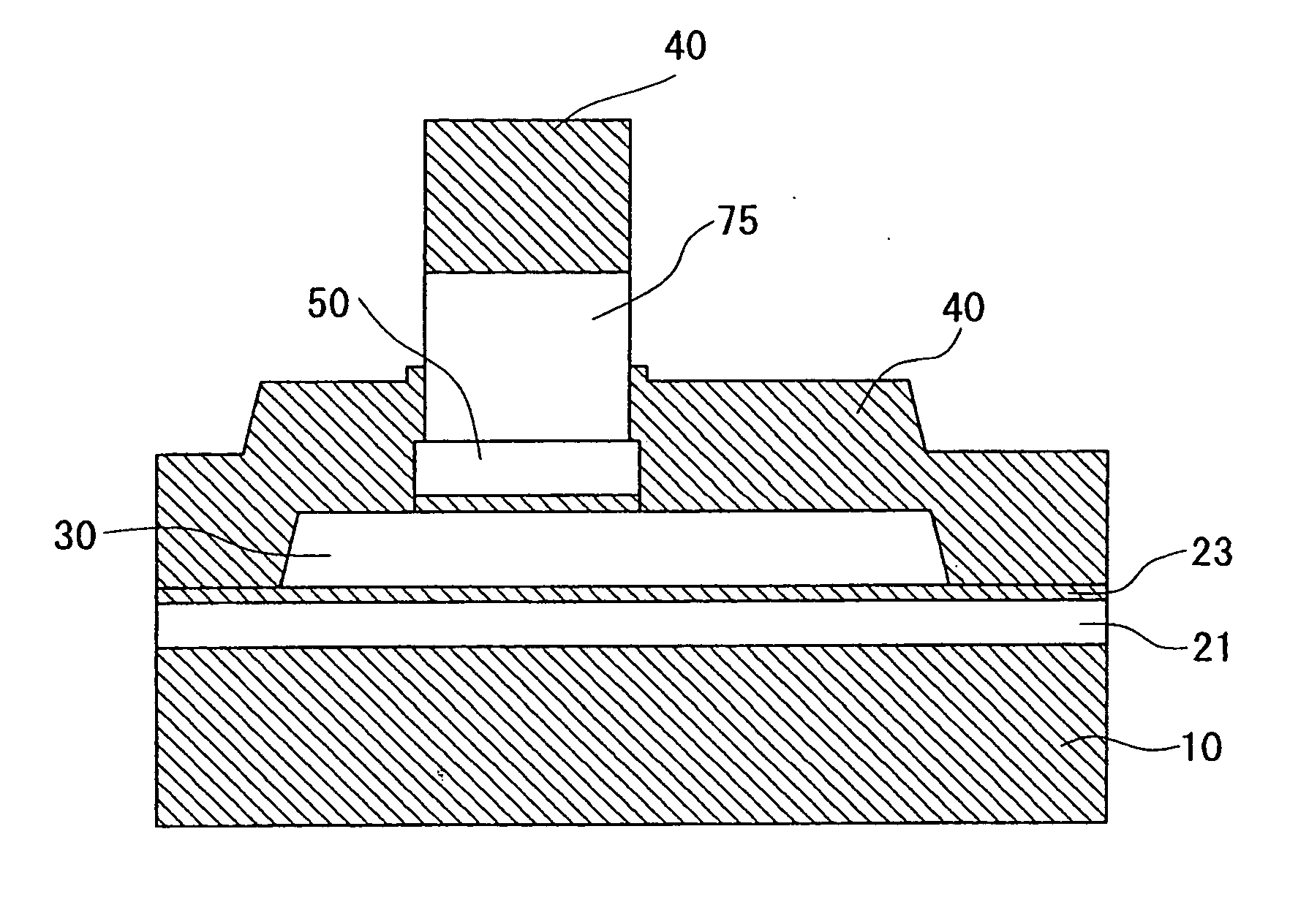
[0049] As a thin layer device of the present invention, a thin layer device having an epitaxial NbN / MgO / NbN-SIS junction as a multilayer structure substance on a SiO2 substrate was produced.

[0050] First of all, an NbN thin film was epitaxially grown up to 100 nm thickness on an MgO temporary substrate having a thickness of 300 μm, then on the NbN thin film, an epitaxial MgO thin film in a thickness of 20 nm, was further formed as an etching protecting layer, by an RF sputtering method and a DC reactive sputtering method.

[0051] Furthermore, on this MgO thin film which is an etching protecting layer, a lower electrode layer in a thickness of 200 nm was formed by epitaxial growth, then an MgO layer in a thickness of about 0.7 nm was formed by an RF sputtering method, and an NbN layer in a thickness of 200 nm was formed by epitaxial growth as an upper electrode layer. Based on this, an epitaxial NbN / MgO / NbN-SIS junction was produced, and then the MgO thin layer at the peripheral of th...

example 2

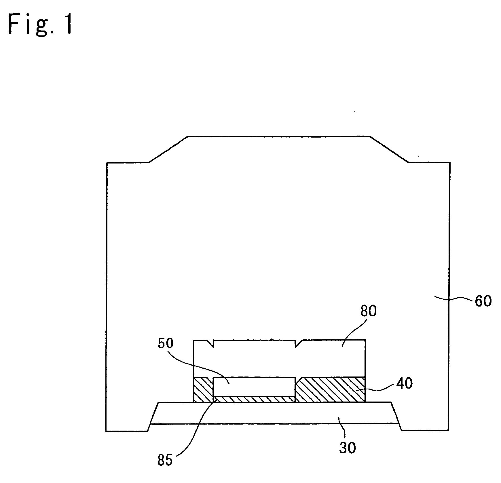
[0053] As a thin layer device of the present invention, an SIS mixer for an 870 GHz band waveguide was produced. A microscopic photo of the resultant SIS mixer for a waveguide is shown in FIG. 10. FIGS. 10(a) and (b) are cross-sectional views, obtained by using a dicing saw, of an SIS mixer for a waveguide on a SiO2 substrate, and FIG. 10(c) shows a transmitted observation of the SIS mixer part from the side of the SiO2 substrate having a thickness of about 20 μm.

[0054]FIG. 11 shows evaluation results of warpage and substrate cross-section of the SiO2 substrate of the resultant SIS mixer for a waveguide. As shown in FIG. 11(a), a rising central part of about 0.7 μm higher than the peripheral part was confirmed as evaluation result of substrate warpage in about 1 mm length zone. This means presence of small stress inside the substrate and having excellent flatness.

[0055]FIG. 11(b) shows measurement result of SiO2 substrate thickness by a laser microscope. Substrate thickness was ab...


PUM


Abstract

A method for producing a thin layer device such as a superconductive device excellent in mechanical strength and useful as a submillimeter band receiver is provided. The thin layer device is produced by forming a multilayer structure substance comprising an NbN / MgO / NbN-SIS junction on an MgO temporary substrate, then forming SiO2, as a substrate, on said multilayer structure substance, and subsequently removing the MgO temporary substrate by etching. A superconductive device (a thin layer device) produced by a method of the present invention has excellent performance and high mechanical strength, and therefore introduction to a waveguide for a submillimeter band is also easy.

Description

BACKGROUND OF THE INVENTION [0001] 1. Field of the Invention: [0002] The present invention relates to a method for fabricating a thin layer device, and in more detail the present invention relates to a method for fabricating a thin layer device such as a superconductive device having an SIS junction on a SiO2 substrate, and a superconductive device. [0003] 2. Description of the Related Art: [0004] In the fields of global environment measurement or radio astronomy and the next generation wireless communication, development of a receiver or oscillator for a submillimeter band has been desired, and research and development of a superconductive device such as the Josephson junction has been made as an example. A superconductive SIS (Superconductor-Insulator-Superconductor) junction which is one of the Josephson junction flows superconductive tunneling current between two superconductive electrodes up to a critical current, while generation of voltage between two superconductive electrod...

Claims


Application Information

Patent Timeline
IPC IPC(8): H01L21/30H01L21/00
CPCH01L39/223H01L39/2493Y10S438/977H10N60/12H10N60/0912
Inventor KAWAKAMI, AKIRA
Owner NAT INST OF INFORMATION & COMM TECH
Why Eureka
Try Eureka