CMOS amplifier
a technology of amplifier and amplifier, which is applied in the direction of amplifier with semiconductor device/discharge tube, dc-amplifiers with dc-coupled stages, etc., can solve the problems of low power consumption, equipment cannot be designed, and their configurations become complex
- Summary
- Abstract
- Description
- Claims
- Application Information
AI Technical Summary
Benefits of technology
Problems solved by technology
Method used
Image

Examples
first embodiment
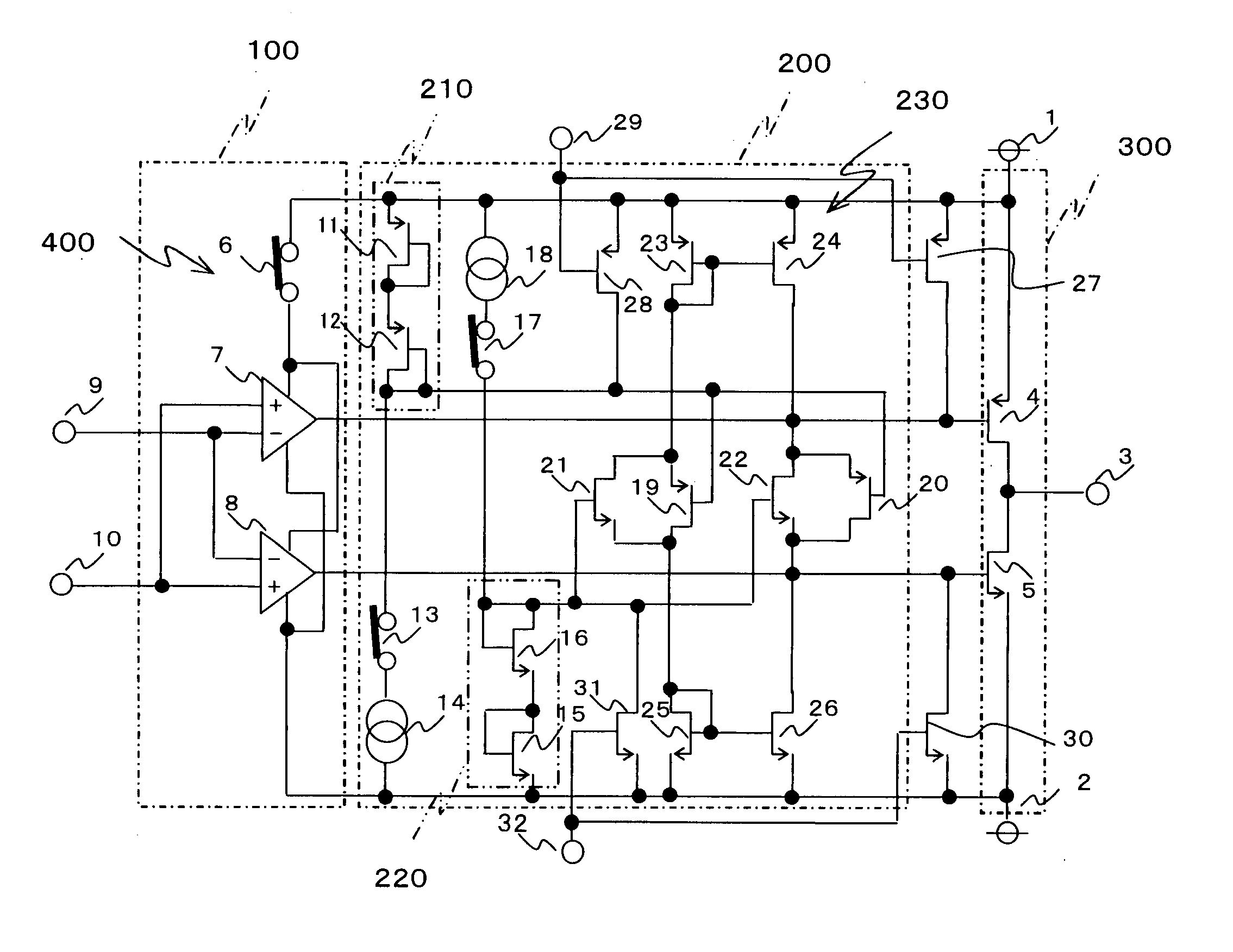
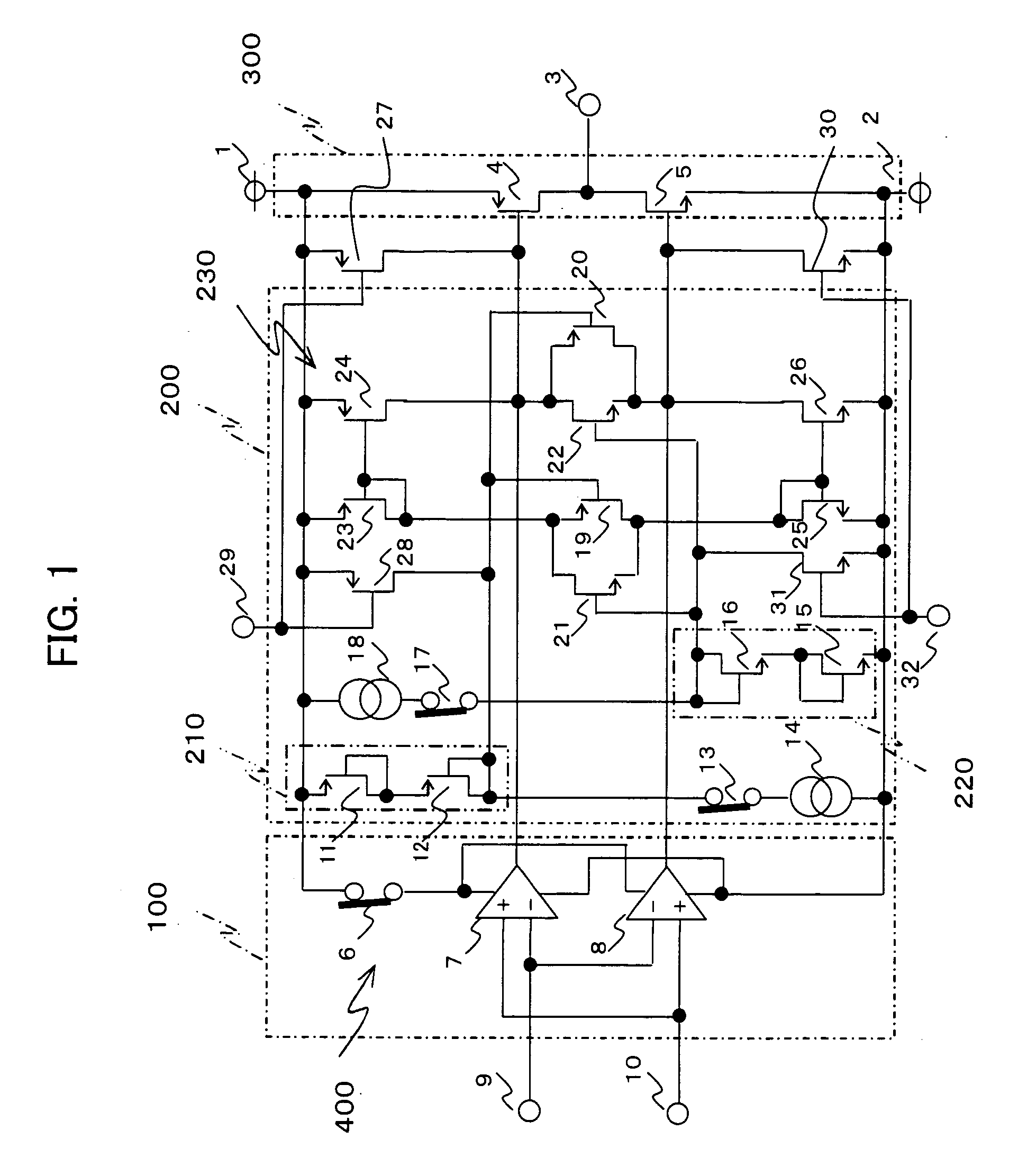
[0037]FIG. 1 is a circuit diagram showing the configuration of a CMOS amplifier according to the first embodiment of the invention. In a push-pull type output stage 300 of FIG. 1, a grounded-source push-pull circuit, which comprises a P-channel MOS transistor 4 for push side output and a N-channel MOS transistor 5 for pull side output, is connected between a plus power supply terminal 1 serving as a first power supply terminal and a minus power supply terminal (or a GND terminal) 2 serving as a second power supply terminal.
[0038] A differential type input stage 100 comprises first and second differential amplifier circuits 7 and 8. The differential amplifier circuits 7 and 8 amplify signals inputted from a plus input terminal 9 and a minus input terminal 10 to drive the P-channel MOS transistor 4 and the N-channel MOS transistor 5 respectively. As a result, signals produced by amplifying the signals inputted from the plus input terminal 9 and the minus input terminal 10 are outputt...
second embodiment
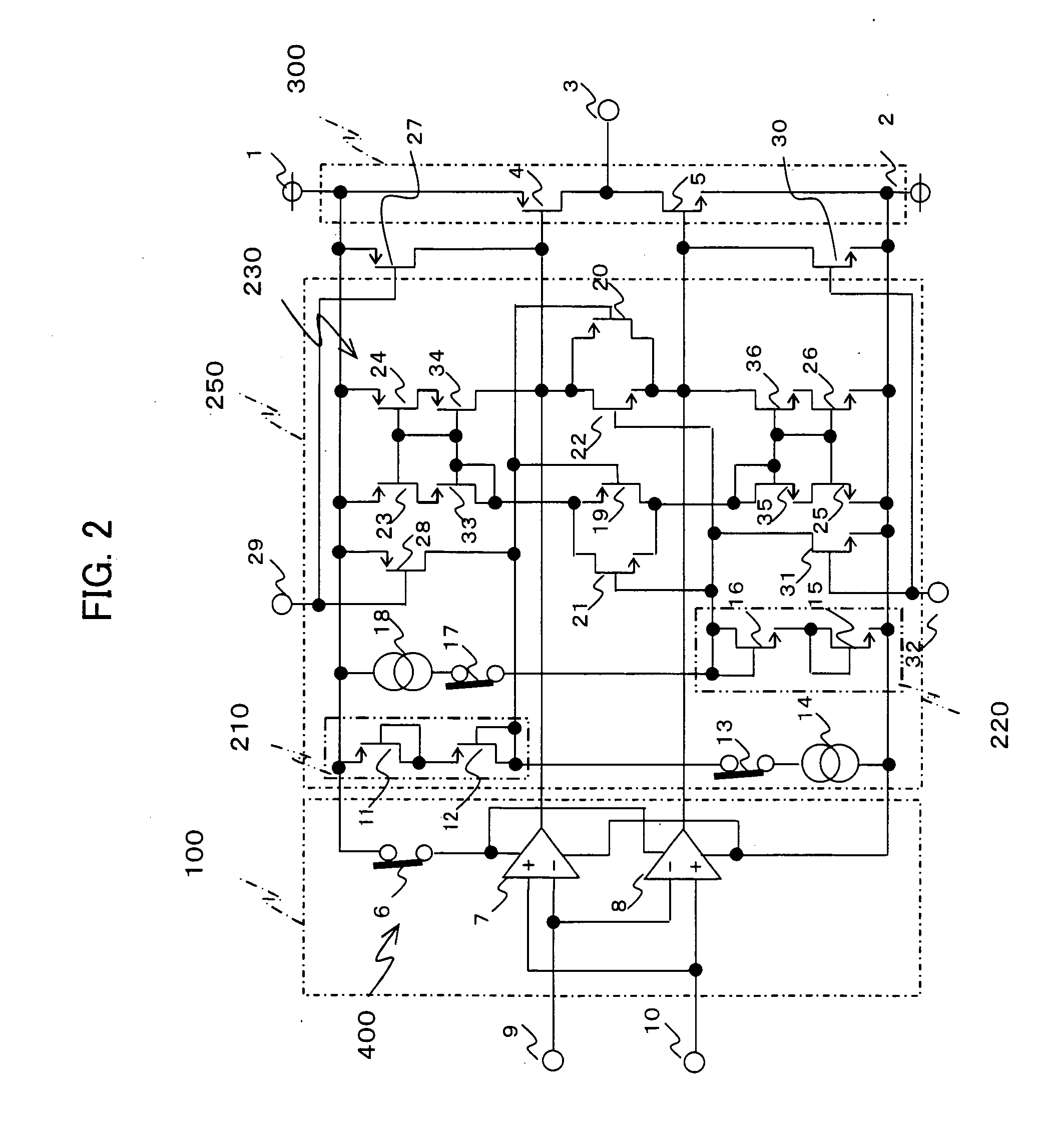
[0065]FIG. 2 is a circuit diagram showing the configuration of a CMOS amplifier according to a second embodiment of the invention. As shown in FIG. 2, in the second embodiment, an idling current control circuit 250 is used instead of the idling current control circuit 200. In the idling current control circuit 250, P-channel MOS transistors 33 and 34 are cascode-connected to the P-channel MOS transistors 23 and 24 respectively, and N-channel MOS transistors 35 and 36 are cascode-connected to the N-channel MOS transistors 25 and 26 respectively; however, the configuration other than those is the same as that shown in FIG. 1.
[0066] Specifically describing, the tenth and eleventh P-channel MOS transistors 33 and 34 are cascode-connected to the sixth and seventh P-channel MOS transistors 23 and 24 respectively and the gates of the tenth and eleventh P-channel MOS transistors 33 and 34 are connected in common with the gates of the sixth and seventh P-channel MOS transistors 23 and 24.
[...
third embodiment
[0070]FIG. 3 is a circuit diagram showing the configuration of a CMOS amplifier according to a third embodiment of the present invention. As shown in FIG. 3, the third embodiment differs from the first embodiment in that a resistor 37 is inserted between the output terminal 3 and a GND (grounding) terminal 38.
[0071] By using such a configuration, a potential at the output terminal 3 is fixed at a GND potential in the stand-by state, and therefore no unfixed potential is generated. As a result, defects such as leakage of current can be detected at the P-channel MOS transistor 4 for the push side output and the N-channel MOS transistor 5 for the pull side output. The configuration other than the above is the same as that shown in FIG. 1.
[0072] With this embodiment, the defects, such as leakage of current, caused at the transistors are detected as follows: if a leakage current Ip has occurred at the P-channel MOS transistor 4, a DC voltage at the output terminal 3 reaches R37×Ip (whe...
PUM
 Abstract
Description
Claims
Application Information
 - R&D
- Intellectual Property
- Life Sciences
- Materials
- Tech Scout
- Unparalleled Data Quality
- Higher Quality Content
- 60% Fewer Hallucinations
Browse by: Latest US Patents, China's latest patents, Technical Efficacy Thesaurus, Application Domain, Technology Topic, Popular Technical Reports.
© 2025 PatSnap. All rights reserved.Legal|Privacy policy|Modern Slavery Act Transparency Statement|Sitemap|About US| Contact US: help@patsnap.com