
Semiconductor electrode, fabrication method thereof and solar cell comprising the same

a technology of semiconductor solar cells and semiconductor electrodes, which is applied in the direction of electrolytic capacitors, solid-state devices, electrochemical generators, etc., can solve the problems of limited ability to improve the conversion efficiency of solar energy into electrical energy, large and expensive equipment for silicon solar cells, and high fabrication costs, so as to achieve the effect of increasing photoelectric efficiency

Inactive Publication Date: 2007-04-26
SAMSUNG ELECTRONICS CO LTD
View PDF1 Cites 19 Cited by
  • Summary
  • Abstract
  • Description
  • Claims
  • Application Information

AI Technical Summary

Benefits of technology

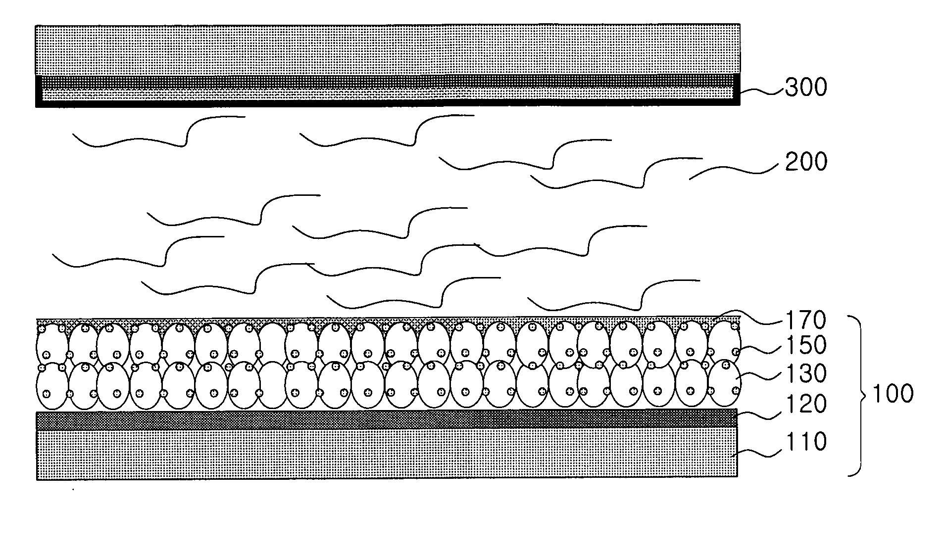
[0012] Accordingly, the present invention has been made keeping in mind the above problems occurring in the related art, and exemplary embodiments of the present invention provide a semiconductor electrode, in which back transfer of electrons in an excited state is prevented, thus increasing photoelectric efficiency.
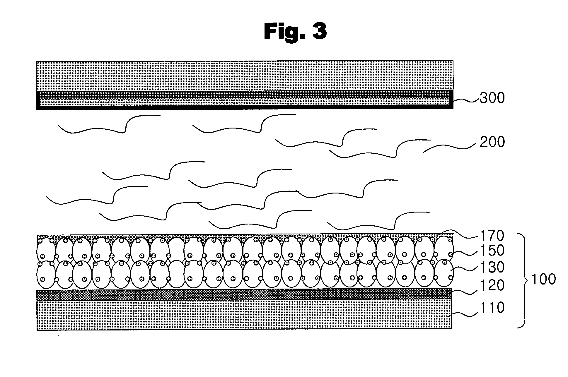
[0014] Further exemplary embodiments of the present invention provide a solar cell having high efficiency, and which includes the exemplary embodiment of a semiconductor electrode.

Problems solved by technology

However, the silicon solar cell requires the use of large and expensive equipment, and expensive materials leading to high fabrication costs.
Further, the ability to improve the conversion efficiency of solar energy into electrical energy is limited.
However, according to the above method, less of an interaction between the dye molecules results not in prevention of back electron transfer in the semiconductor electrode, but merely in exhibition of the inherent function of the dye as a photosensitizer.
Thus, an effect of improving the photoelectric efficiency is limited.

Method used


Image

  • Semiconductor electrode, fabrication method thereof and solar cell comprising the same
  • Semiconductor electrode, fabrication method thereof and solar cell comprising the same
  • Semiconductor electrode, fabrication method thereof and solar cell comprising the same

Examples


example 1

[0069] After fluorine-doped tin oxide (FTO) was applied on a glass substrate using a sputter, a paste of TiO2 particles having a diameter of 13 nm was applied using a screen printing process and then dried at 70° C. for 30 minutes. Subsequently, the dried substrate was placed into an electrical furnace, after which the temperature of the furnace was increased at a rate of 3° C. / min. in a normal atmosphere and thus the substrate was maintained at 450° C. for 30 minutes and then cooled at the same rate as that applied when increasing the temperature, therefore obtaining a porous TiO2 film of about 15 μm thick.

[0070] Subsequently, the glass substrate having the metal oxide layer formed thereon was immersed in an ethanol solution of 0.3 mM cis-bis(isothiocyanato)bis(2,2′-bipyridyl-4,4′-dicarboxylato)-ruthenium (‘N3 dye’), represented by Formula 3 below, for 24 hours and then dried, thereby adsorbing the dye on the surface of the TiO2 layer. After the completion of the adsorption of the...

example 2

[0072] A semiconductor electrode was fabricated in the same manner as in Example 1, with the exception that 4-ethoxysalicylic acid (0.1 mmol, 18.2 mg) was used instead of 4-hydroxybenzoic acid.

example 3

[0073] A semiconductor electrode was fabricated in the same manner as in Example 1, with the exception that 5-(4-methoxyphenyl)1,3,4-oxydazole-2-thiol (0.1 mmol, 20.8 mg) was used instead of 4-hydroxybenzoic acid.


PUM


Abstract

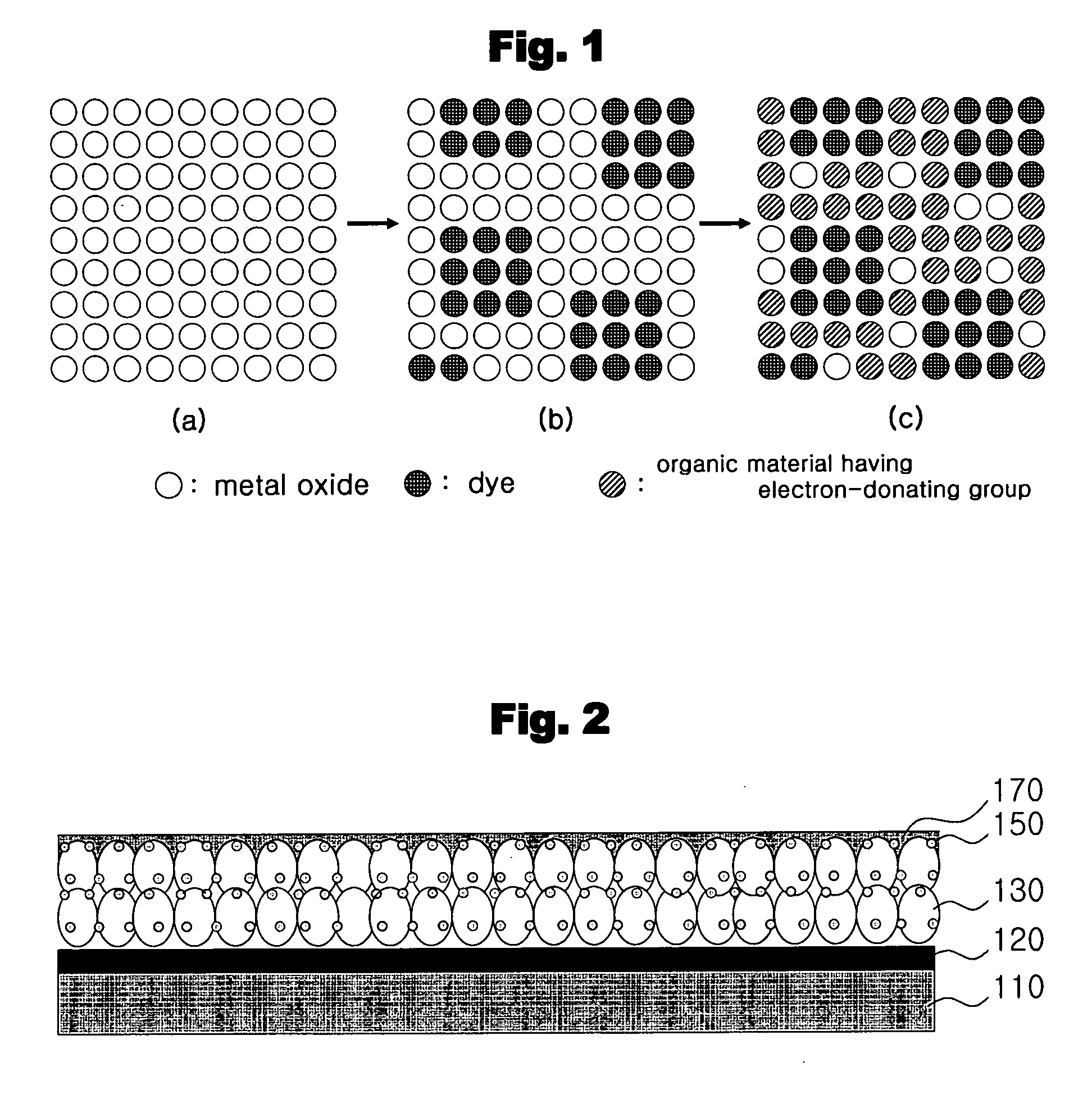
A semiconductor electrode, a fabrication method thereof and a solar cell including the semiconductor electrode each include a metal oxide layer of metal oxide nanoparticles having dye molecules adsorbed thereon. In the semiconductor electrode of the present invention, the surface of the metal oxide layer is treated with an aromatic or heteroaromatic organic material having an electron-donating group. Thus, since the semiconductor electrode can provide an effect of improving photoelectric efficiency by virtue of an increase in short-circuit photocurrent density and open-circuit voltage, it can be applied to a high efficiency solar cell.

Description

[0001] This application claims priority to Korean Patent Application No. 2005-99531, filed on Oct. 21, 2005 and all the benefits accruing therefrom under 35 U.S.C. § 119, and the contents of which in its entirety are herein incorporated by reference. BACKGROUND OF THE INVENTION [0002] 1. Field of the Invention [0003] The present invention relates, generally, to a semiconductor electrode, a fabrication method thereof, and a solar cell comprising the same, and more particularly, to a semiconductor electrode, in which the surface of metal oxide having a dye adsorbed thereon is treated with an aromatic or heteroaromatic organic material having an electron-donating group, thus increasing the photoelectric efficiency of a solar cell, and to a method of fabricating such a semiconductor electrode and a solar cell comprising the semiconductor electrode. [0004] 2. Description of the Related Art [0005] In general, a solar cell, which is a photoelectric conversion device for converting solar li...

Claims


Application Information

Patent Timeline
IPC IPC(8): H01L31/00
CPCH01G9/2031H01L51/0086H01M14/005Y02E10/542H10K85/344H01L31/04H01L31/0224
Inventor JUNG, WON CHEOLNAM, JUNG GYUPARK, SANG CHEOLSOHN, BYUNG HEE
Owner SAMSUNG ELECTRONICS CO LTD
Learn More