Processing apparatus
a technology of processing apparatus and filter, which is applied in the direction of crystal growth process, after-treatment details, solid state diffusion coating, etc., can solve the problems of difficult to control the radical flux to an ultra-low level, and the method of controlling the radical flux has some negative effects
- Summary
- Abstract
- Description
- Claims
- Application Information
AI Technical Summary
Benefits of technology
Problems solved by technology
Method used
Image
Examples
first exemplary embodiment
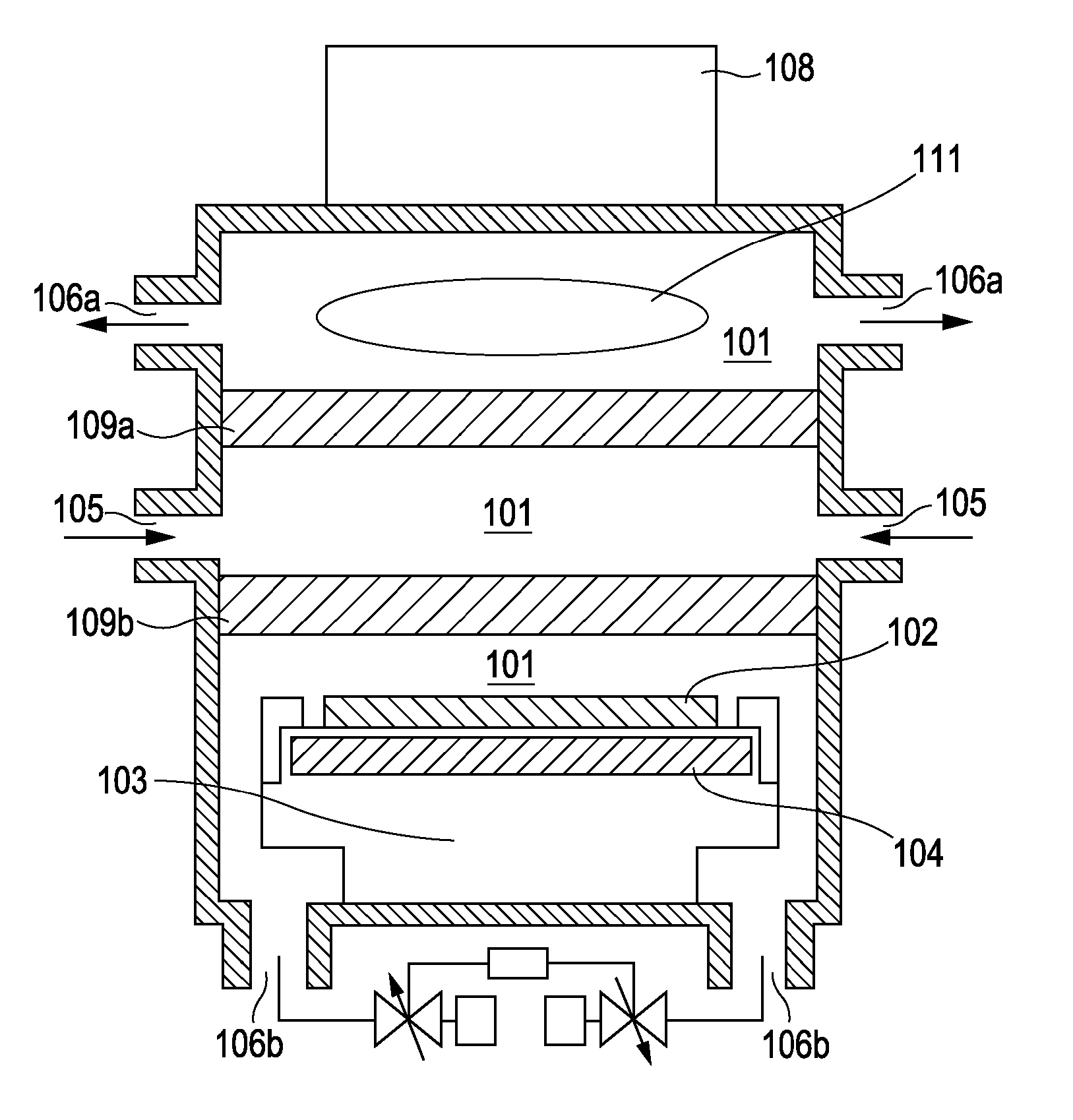
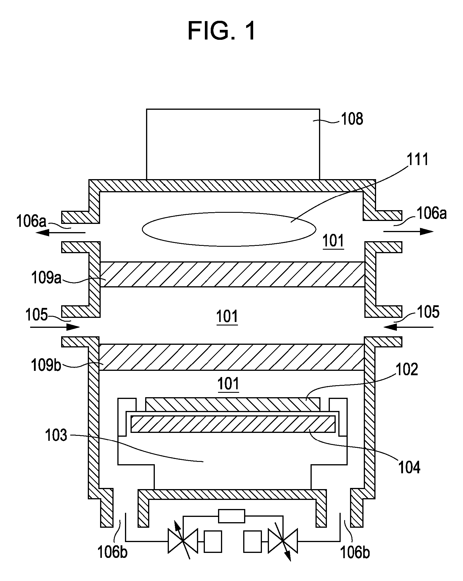
[0041] A processing apparatus according to a First Exemplary Embodiment of the present invention will be described with reference to FIG. 1.
[0042] In a treatment chamber 101, a surface of a substrate 102 such as a semiconductor is processed with radicals. A radical-forming unit 108 generates radicals in a radical-generating region 111 located in the upper region of the treatment chamber 101.
[0043] Gas inlets 105 are disposed at the lower side with respect to the radical-forming unit 108 and serve as mechanisms for introducing a reaction gas into the treatment chamber 101.
[0044] A substrate-support 103 is disposed at the lower side with respect to the gas inlets 105 and supports the substrate 102 to be processed.
[0045] In the First Exemplary Embodiment, the gas inlets 105 are disposed at the lower side with respect to the radical-forming unit 108, and the substrate-support 103 is disposed at the lower side with respect to the gas inlets 105. However, these positions can be change...
second exemplary embodiment
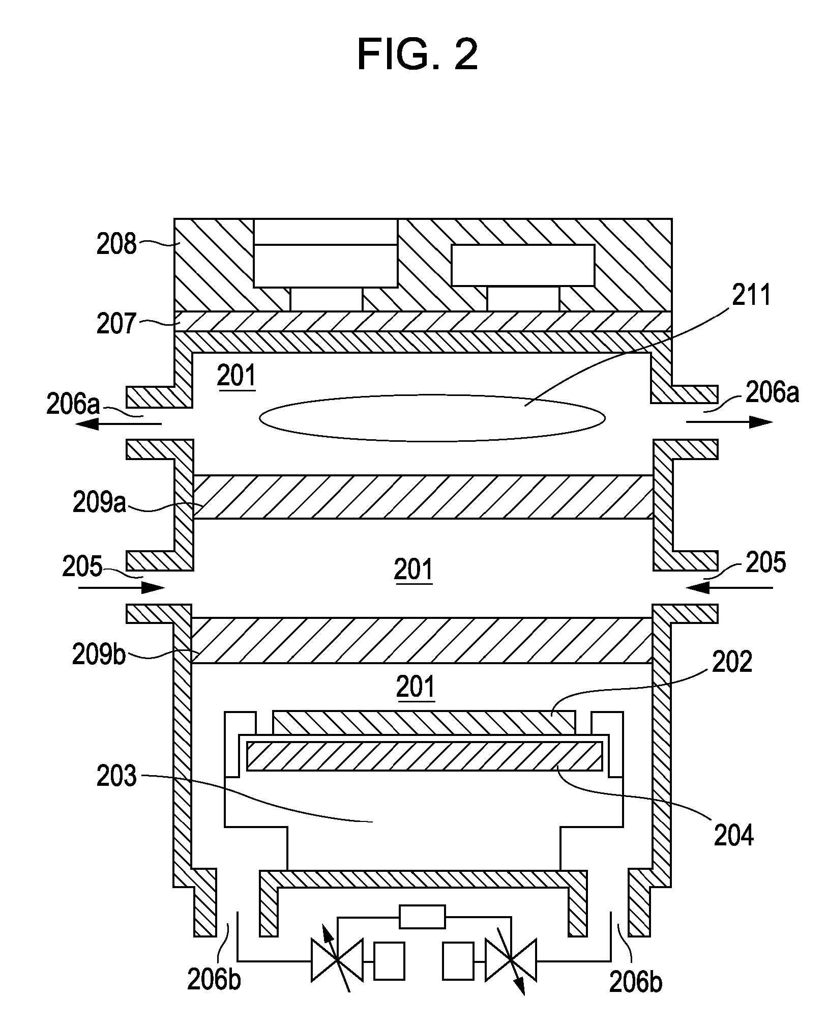
[0101] A microwave excitation surface-wave interfered plasma-processing apparatus using an endless circular waveguide with slots according to a Second Exemplary Embodiment of the present invention will now be described with reference to FIG. 2.
[0102] In a radical-treatment chamber 201, a surface of a substrate 202 such as a semiconductor is processed with radicals.
[0103] An endless circular waveguide 208 with slots serves as a radical-forming mechanism and also serves as a mechanism for introducing a microwave to the treatment chamber 201 through a microwave-transmitting unit 207.
[0104] The endless circular waveguide 208 with slots forms radicals in a radical-generating region 211 at the upper region of the treatment chamber 201.
[0105] Gas inlets 205 are disposed at the lower side with respect to the endless circular waveguide (radical-forming mechanism) 208 and serve as a mechanism for introducing a reaction gas into the treatment chamber 201.
[0106] A substrate-support 203 is ...
third exemplary embodiment
[0183] A UV-excitation radical processing apparatus according to a Third Exemplary Embodiment of the present invention will now be described with reference to FIG. 3.
[0184] In a treatment chamber 301, a surface of a substrate 302 such as a semiconductor is processed with radicals. A UV light source serving as a radical-forming unit 308 emits UV light by an application of power. The reaction gas is excited by the UV light to generate radicals in a radical-generating region 311 at the upper portion of the treatment chamber 301.
[0185] Gas inlets 305 are disposed at the lower side with respect to the radical-forming unit 308 and serve as a mechanism for introducing a reaction gas into the treatment chamber 301.
[0186] A substrate-support 303 is disposed at the lower side with respect to the gas inlets 305 and supports a substrate 302 to be processed.
[0187] A heater 304 controls the temperature of the substrate 302 disposed on the substrate-support 303.
[0188] First gas outlets 306a a...
PUM
| Property | Measurement | Unit |
|---|---|---|
| Temperature | aaaaa | aaaaa |
| Electrical conductance | aaaaa | aaaaa |
| Distance | aaaaa | aaaaa |
Abstract
Description
Claims
Application Information
 - R&D Engineer
- R&D Manager
- IP Professional
- Industry Leading Data Capabilities
- Powerful AI technology
- Patent DNA Extraction
Browse by: Latest US Patents, China's latest patents, Technical Efficacy Thesaurus, Application Domain, Technology Topic, Popular Technical Reports.
© 2024 PatSnap. All rights reserved.Legal|Privacy policy|Modern Slavery Act Transparency Statement|Sitemap|About US| Contact US: help@patsnap.com


