
Systems, circuits and methods for extending the detection range of an inspection system by avoiding circuit saturation

a technology of circuits and inspection systems, applied in the direction of photoelectric discharge tubes, electron multiplier details, instruments, etc., to achieve the effect of extending the detection range of inspection systems, sufficient resolution, and low resolution

Active Publication Date: 2007-01-18
KLA TENCOR TECH CORP
View PDF28 Cites 28 Cited by
  • Summary
  • Abstract
  • Description
  • Claims
  • Application Information

AI Technical Summary

Benefits of technology

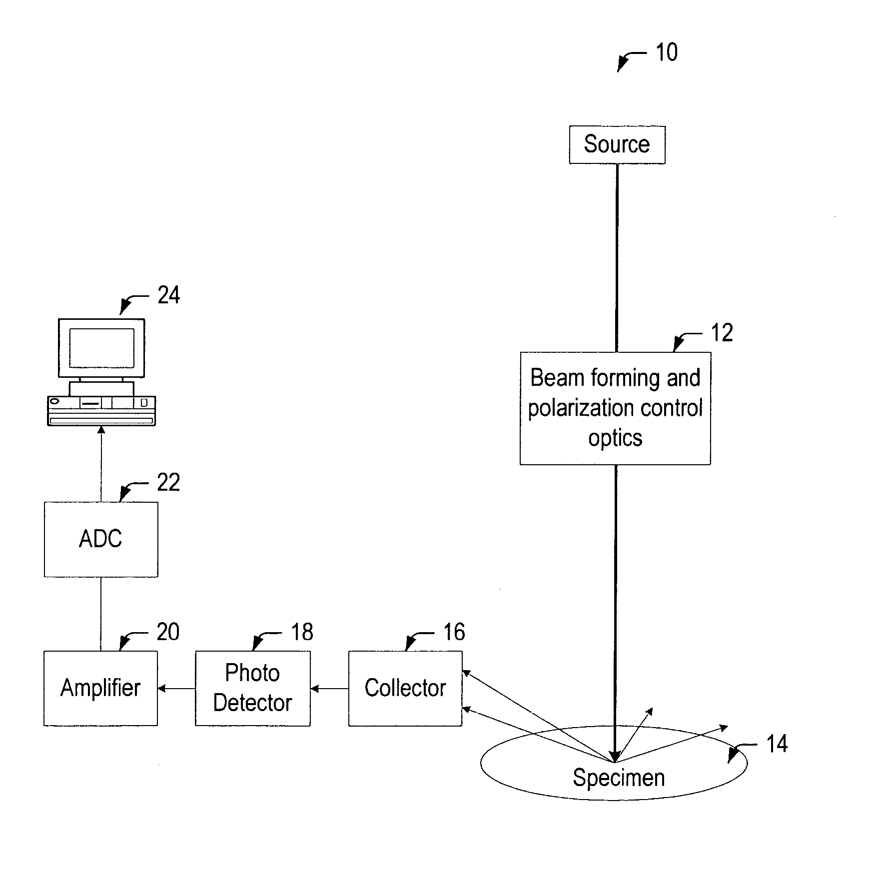
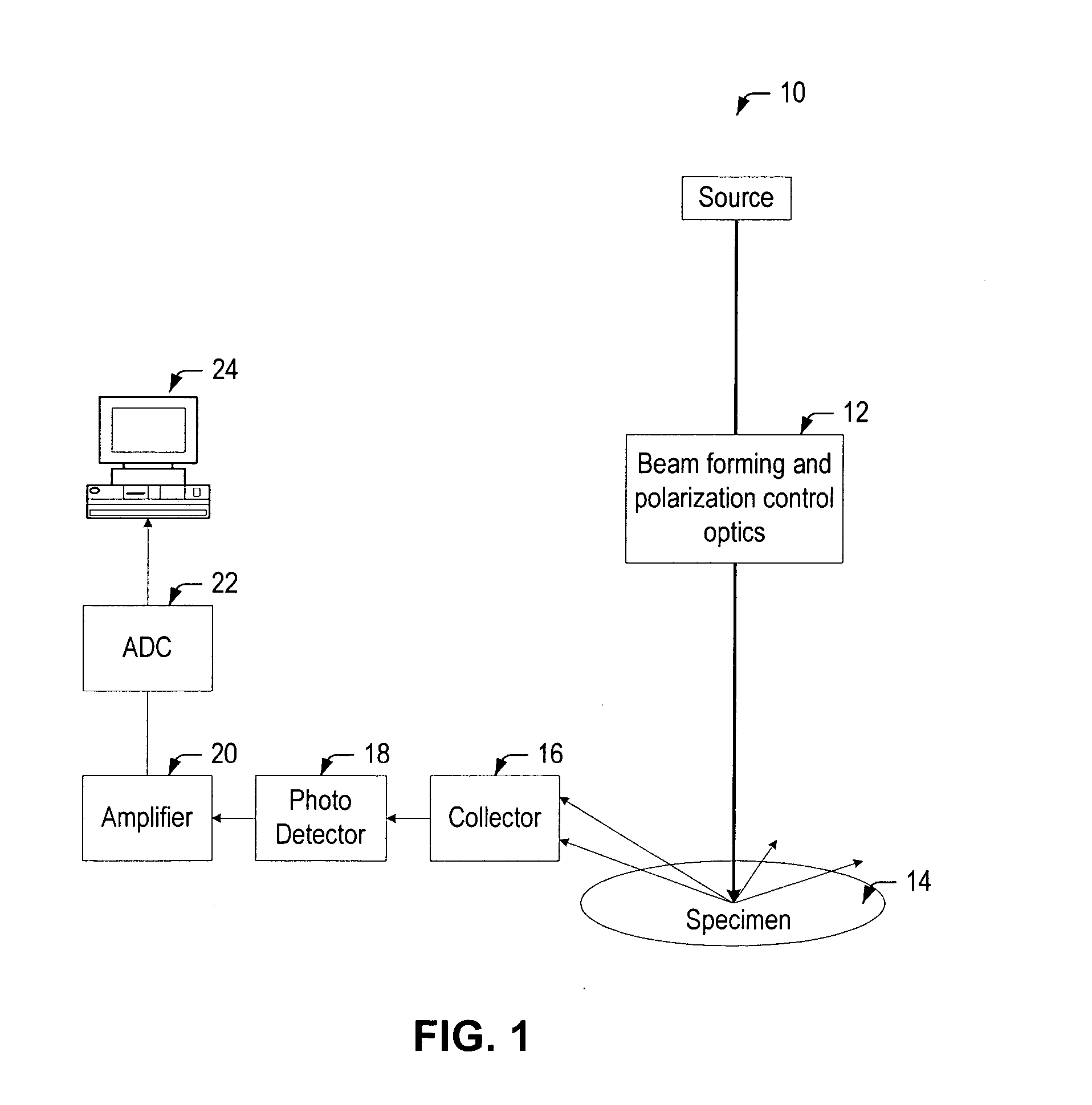
[0014] The inspection systems, circuits and methods described herein enhance defect detection by addressing saturation levels of the amplifier and analog-digital circuitry as a limiting factor of the measurement detection range of an inspection system. In accordance with one embodiment of the invention, a method for inspecting a specimen includes directing light to the specimen and detecting light scattered from the specimen. However, unlike prior art inspection systems, the step of detecting may use only one photodetector for detecting the light scattered from the specimen and for converting the light into an electrical signal. The step of detecting may also include generating a first signal and a second signal in response to the electrical signal, where the second signal differs from the first. For example, the first signal may be generated to have a higher resolution than the second signal for detecting substantially lower levels of the scattered light. In most cases, the method may use the first signal for detecting features, defects or light scattering properties of the specimen until the first signal reaches a predetermined threshold value. Once the predetermined threshold value is reached, however, the method may use the second signal for said detecting.
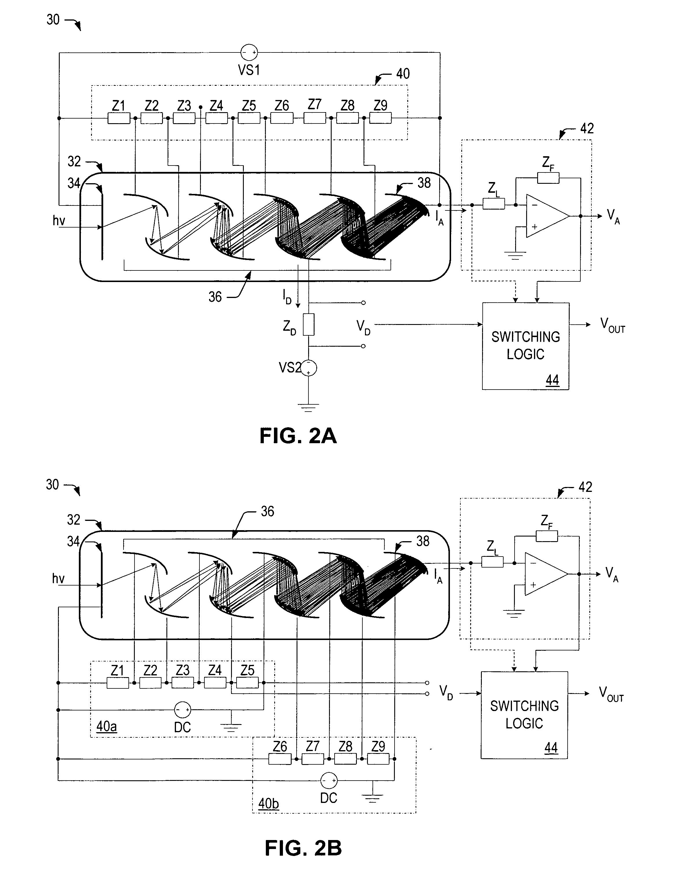
[0015] Compared to the first signal, the second signal may be generated with a substantially lower resolution for detecting substantially higher levels of the scattered light. As such, the method described herein may extend the measurement detection range of an inspection system by switching to the second (lower resolution) signal once the first (higher resolution) signal reaches the predetermined threshold value. In other words, the circuits, systems and methods described herein may be used to provide at least two detection ranges, one for detecting lower levels of light and one for detecting higher levels of light. Sufficient resolution may be maintained at the “switch point” by overlapping the detection ranges to some degree.
[0017] The circuit may also include an amplifier stage for generating at least a first signal and a second signal in response to the electrical signal produced by the photodetector. As noted above, the first signal may be generated with a higher resolution for detecting substantially lower levels of the scattered light. On the other hand, the lower resolution the second signal may enable substantially higher levels of the scattered light to be detected without saturating the amplifier and analog-digital circuitry of the inspection system. Thus, saturation may be avoided by dynamically switching to the second signal once the first signal becomes high enough to cause the amplifier and / or analog-digital circuitry to saturate. Though exemplary embodiments are described below in the context of a “dual-output amplifier,” the amplifier stage described herein may be modified for generating more than two output signals from the electrical signal produced by the photodetector.

Problems solved by technology

However, unlike prior art inspection systems, the step of detecting may use only one photodetector for detecting the light scattered from the specimen and for converting the light into an electrical signal.

Method used


Image

  • Systems, circuits and methods for extending the detection range of an inspection system by avoiding circuit saturation
  • Systems, circuits and methods for extending the detection range of an inspection system by avoiding circuit saturation
  • Systems, circuits and methods for extending the detection range of an inspection system by avoiding circuit saturation

Examples


Embodiment Construction

[0040] The methods and systems described herein enhance defect detection by addressing various limiting factors of measurement detection range including, but not limited to, detector saturation, amplifier saturation and the fixed bit range of analog-to-digital converters (ADC). Unlike some currently used inspection methods, the inspection system described herein is able to extend the measurement detection range while maintaining signal linearity and stability, and without employing additional detectors, optics and electronic components, all of which undesirably increase space consumption, complexity and cost of the inspection system.

[0041] Various embodiments are described herein for an optical inspection system or tool that may be used for inspecting a specimen. The term “specimen” is used herein to refer to a wafer, a reticle, or any other sample that may be inspected for defects, features, or other information (e.g., an amount of haze or film properties) known in the art.

[0042]...


PUM


Abstract

Inspection systems, circuits and methods are provided to enhance defect detection by addressing saturation levels of the amplifier and analog-digital circuitry as a limiting factor of the measurement detection range of an inspection system. In accordance with one embodiment of the invention, a method for inspecting a specimen includes directing light to the specimen and detecting light scattered from the specimen. However, the step of detecting may use only one photodetector for detecting the light scattered from the specimen and for converting the light into an electrical signal. The step of detecting also includes generating a first signal and a second signal in response to the electrical signal, where the second signal differs from the first. For example, the first signal may be generated to have a higher resolution than the second signal for detecting substantially lower levels of the scattered light. In most cases, the method may use the first signal for detecting features, defects or light scattering properties of the specimen until the first signal reaches a predetermined threshold value. Once the predetermined threshold value is reached, however, the method may use the second signal for said detecting.

Description

BACKGROUND OF THE INVENTION [0001] 1. Field of the Invention [0002] The present invention generally relates to circuits, systems and methods for extending a measurement detection range of an inspection system used for inspecting a specimen. More specifically, the present invention relates to circuits, systems and methods for extending the measurement detection range of an inspection system by addressing the saturation of the amplifier and analog-digital circuitry as a limiting factor of the measurement detection range. [0003] 2. Description of the Related Art [0004] Fabricating semiconductor devices, such as logic, memory and other integrated circuit devices, typically includes processing a specimen such as a semiconductor wafer using a number of semiconductor fabrication processes to form various features and multiple levels of the semiconductor devices. For example, lithography is a semiconductor fabrication process that typically involves transferring a pattern to a resist arrang...

Claims


Application Information

Patent Timeline
IPC IPC(8): H03F3/08H01J40/14
CPCH03F3/08H01J43/025H01J43/18H01J43/30
Inventor WOLTERS, CHRISTIAN H.ROMANOVSKY, ANATOLYSLOBODOV, ALEXANDER
Owner KLA TENCOR TECH CORP
Learn More