Optimized photomasks for photolithography
a photolithography and photolithography technology, applied in the field of masks, can solve problems such as sub-optimal designs, patterns may not print correctly at all, and unwanted distortions and artifacts accompanied by
- Summary
- Abstract
- Description
- Claims
- Application Information
AI Technical Summary
Benefits of technology
Problems solved by technology
Method used
Image
Examples
Embodiment Construction
)
[0029] As understood herein, the term “wafer pattern” is understood to include any polygon (rectilinear or non-rectilinear) or other shape or pattern to be formed on a semiconductor or other material substrate, for example digital or analog circuit structures or interconnect.
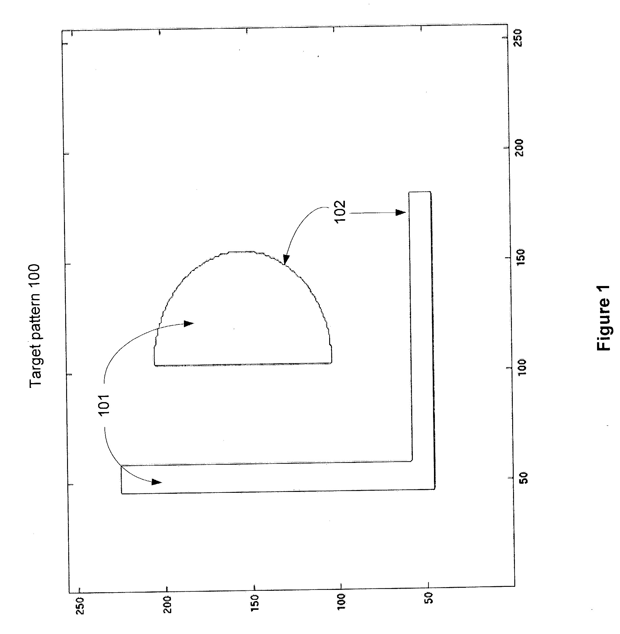
[0030]FIG. 1 is a diagram illustrating an example target pattern 100 to be printed on a wafer using a photolithography process. Target pattern 100 comprises regions 101 enclosed by contours 102. Preferably, areas within regions 101 represent photoresist and the area outside regions 101 represents the absence of photoresist.
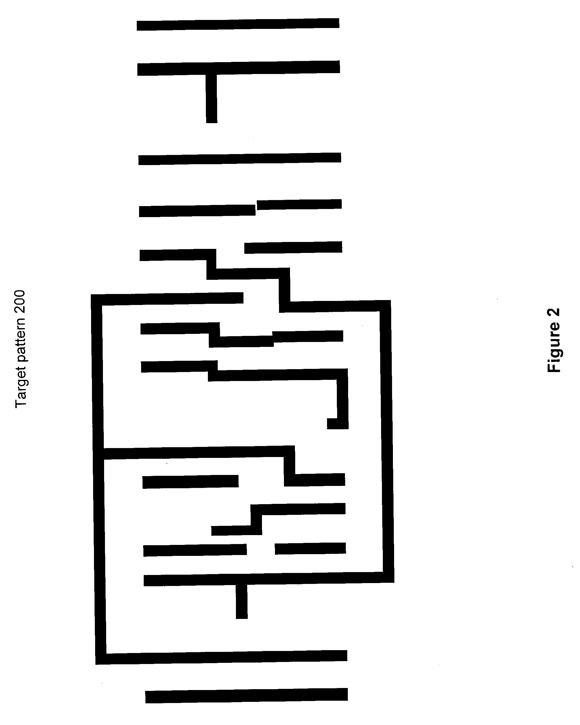
[0031]FIG. 2 is a diagram illustrating a more complex example target pattern 200 to be printed on a wafer using a photolithography process. The complexity of target pattern 200 is more illustrative of a pattern for representing an integrated circuit design.
[0032]FIG. 3 is a diagram illustrating a detail target pattern 300 from the example target pattern 200 of FIG. 2 to be printed on a waf...
PUM
 Abstract
Description
Claims
Application Information
 - R&D
- Intellectual Property
- Life Sciences
- Materials
- Tech Scout
- Unparalleled Data Quality
- Higher Quality Content
- 60% Fewer Hallucinations
Browse by: Latest US Patents, China's latest patents, Technical Efficacy Thesaurus, Application Domain, Technology Topic, Popular Technical Reports.
© 2025 PatSnap. All rights reserved.Legal|Privacy policy|Modern Slavery Act Transparency Statement|Sitemap|About US| Contact US: help@patsnap.com


