Spin injection magnetization reversal element
a technology of spin injection and magnetization, which is applied in the direction of digital storage, instruments, galvano-magnetic devices, etc., can solve the problems of inability to retain magnetization, minute magnetization is unstable, and the resistance of recorded magnetization to thermal agitation is degraded, so as to reduce the critical current density and improve the efficiency of electron spin injection. , the effect of ensuring thermal stability
- Summary
- Abstract
- Description
- Claims
- Application Information
AI Technical Summary
Benefits of technology
Problems solved by technology
Method used
Image
Examples
example 1
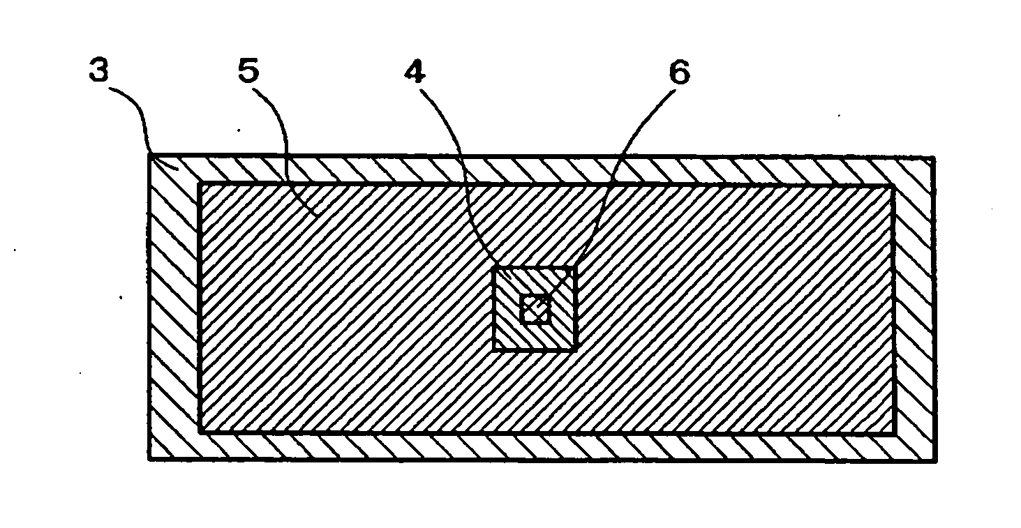
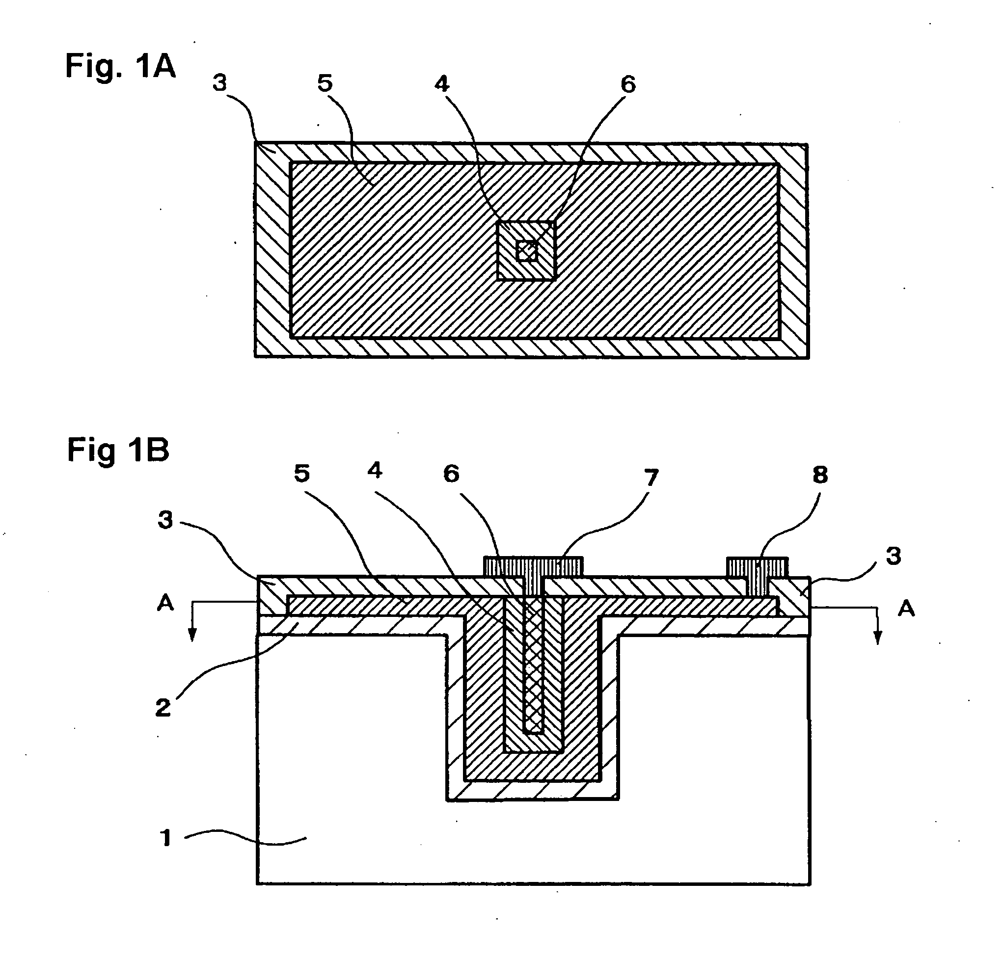
[0054]FIGS. 1A and 1B are views for explaining the arrangement of an element as Example 1 according to the invention, with FIG. 1B being a schematic cross sectional view and FIG. 1A being a schematic cross sectional view taken on line A-A of FIG. 1B. Substrate insulation layer 2 is formed on the surface of substrate 1 formed with a trench structure having a square horizontal cross section. Ferromagnetic fixed layer 5 is arranged on substrate insulation layer 2 while filling the trench structure so as to surround a square-prism-like ferromagnetic free layer 6 with isolation layer 4 in between. Insulation layer 3 is provided over ferromagnetic fixed layer 5, isolation layer 4 and ferromagnetic free layer 6. Ferromagnetic fixed layer 5 is connected to an external power supply (not shown) through fixed layer electrode 8 by way of a through hole opened in insulation layer 3. Ferromagnetic free layer 6 is connected to the external power supply through free layer electrode 7 provided throu...
example 2
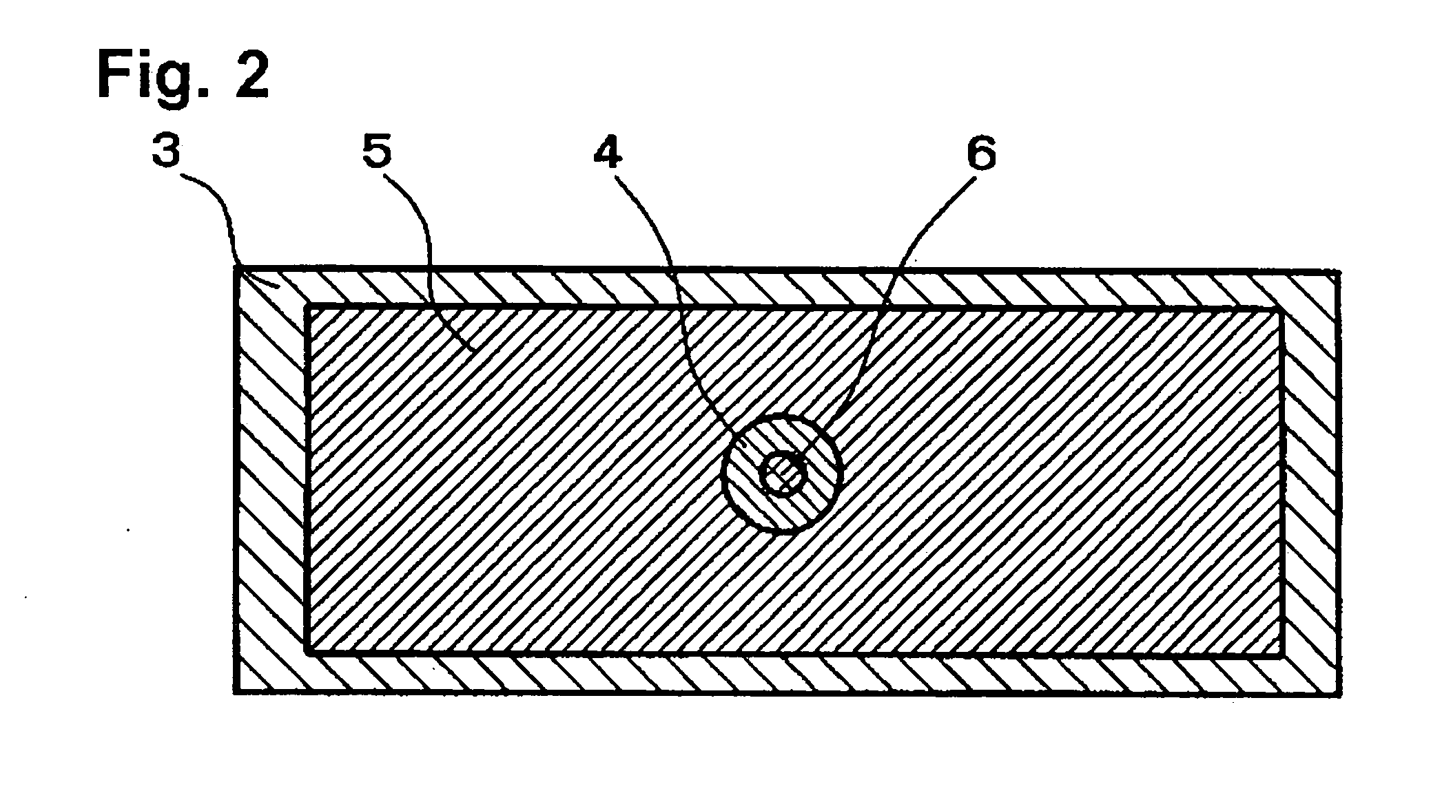
[0058]FIG. 2 is a schematic cross sectional view for explaining the arrangement of an element of Example 2 according to the invention equivalent to the element shown in FIG. 1A. As shown in FIG. 2, the element was fabricated similarly to the element of Example 1, except that a trench structure was formed in a cylinder shape and was provided as Example 2. The shape of ferromagnetic free layer 6 was like a cylinder with a diameter of 10 nm and a depth of 10 nm.
[0059] The operating conditions and characteristics of Example 2 are shown in Table 1. As a result of measuring the resistance values of the element with a detecting current of 300 μA, the resistance value in the high resistance state was 4.6Ω and that in the low resistance state was 4.0Ω.
example 3
[0060] Example 3 is an example in which a laminated electrode was additionally provided for ferromagnetic fixed layer 5 in the element of Example 1 to adjust a resistance value. In each of FIGS. 3A and 3B, there is shown the arrangement of Example 3. FIG. 3B is a schematic cross sectional view for explaining the arrangement of Example 3 and FIG. 3A is a schematic cross sectional view taken on line B-B of FIG. 3B.
[0061] After substrate insulation layer 2 with a silicon oxide film has been formed, the element was fabricated similarly to the element as Example 1 to be obtained as Example 3 except that laminated electrode 9 made of Cu was formed with a thickness of 20 nm and the film thickness of the subsequently formed ferromagnetic fixed layer 5 was made 80 nm.
[0062] The operating conditions and characteristics of Example 3 are shown in Table 1. As a result of measuring the resistance values of the element with a detecting current of 300 μA, the resistance value in the high resistan...
PUM
 Abstract
Description
Claims
Application Information
 - R&D
- Intellectual Property
- Life Sciences
- Materials
- Tech Scout
- Unparalleled Data Quality
- Higher Quality Content
- 60% Fewer Hallucinations
Browse by: Latest US Patents, China's latest patents, Technical Efficacy Thesaurus, Application Domain, Technology Topic, Popular Technical Reports.
© 2025 PatSnap. All rights reserved.Legal|Privacy policy|Modern Slavery Act Transparency Statement|Sitemap|About US| Contact US: help@patsnap.com


