
Low-loss microstrip transmission line structure and a method for its implementation

Inactive Publication Date: 2006-12-21
RPX CORP
View PDF5 Cites 27 Cited by
  • Summary
  • Abstract
  • Description
  • Claims
  • Application Information

AI Technical Summary

Benefits of technology

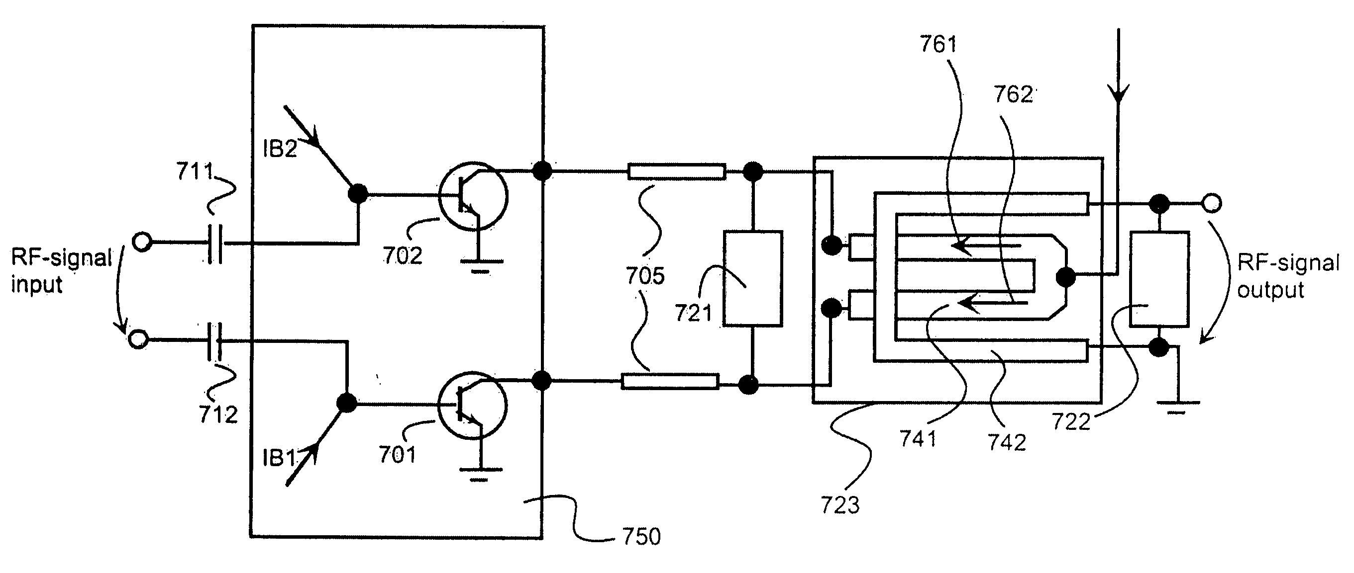
[0020] It is an objective of the present invention to provide a low-loss microstrip transmission line structure for an RF-IC, which microstrip structure avoids the boundary condition associated with the width of the microstrip when targeting a certain level of impedance and / or a certain level of inductive coupling between different strips and which microstrip structure allows the integration of a balun into an RF-IC. It is also an objective of the present invention to remove or mitigate the drawbacks associated with a push-pull power amplifier when using a balun according to the prior art. Furthermore, it is an objective of the present invention to provide a method for implementing a low-loss microstrip transmission line structure into an RF-IC. It is also an objective of the present invention to provide a mobile phone in which the drawbacks associated with a microstrip structure according to the prior art have been removed or mitigated.

Problems solved by technology

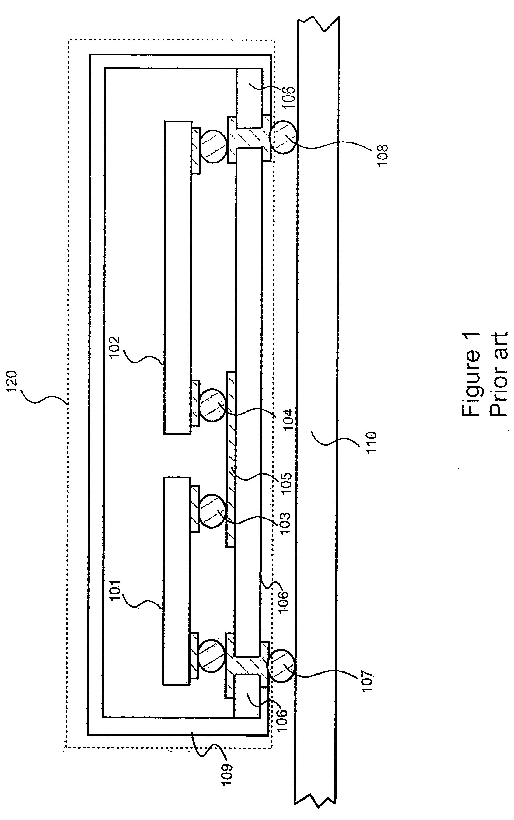
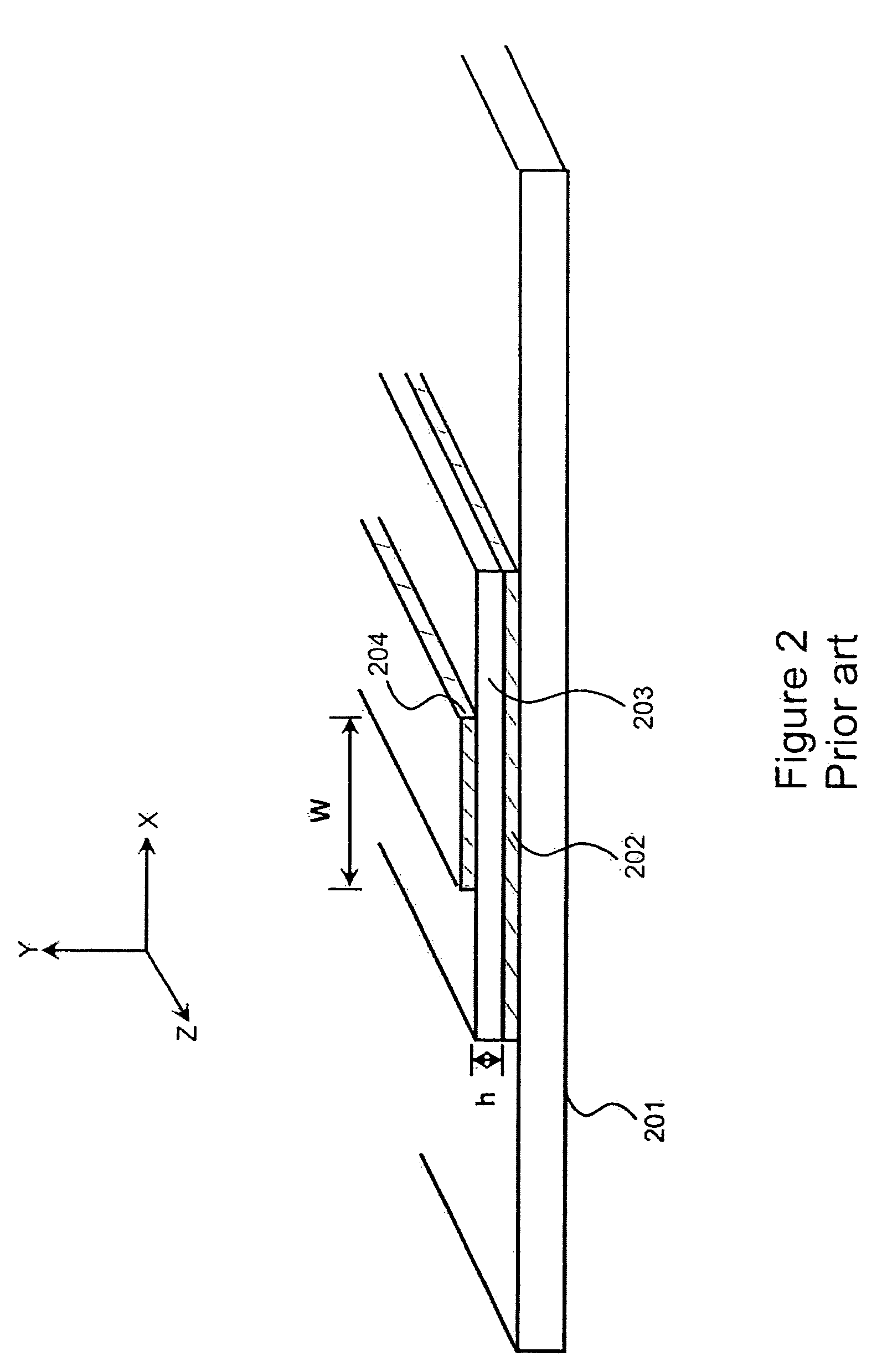
The microstrip structure according to the prior art involves severe drawbacks due to the fact that the thickness of the insulating layer h is limited because of the reasons associated with the manufacturing processes.
The drawback associated with narrowing the microstrip is the fact that the serial resistance grows.
This becomes a problem when the power losses in the system should be low and / or the system should be able to handle high power levels.
When using the microstrip structure according to prior art for integrating a balun into an RF-IC severe drawbacks are, however, introduced.
For instance, if the balun has to be able to handle the power outputted by e.g. a power amplifier in the transmitter of a mobile phone the strips have to be wide enough for being able to carry the power with losses small enough but this would lead to a too low impedance level.
Furthermore, also due to the limitation on the insulator thickness h it is infeasible to arrange a suitable W / h ratio for reaching a sufficient inductive coupling between the microstrips associated with a signal input side and a signal output side of the balun.
The fact that the width of the microstrip W has to be limited if a certain level of impedance is desired and / or the fact that the inductive coupling between different strips is weak has / have also harmful effects when using the prior art microstrip structure for e.g. directional couplers, impedance transformers, and filters.
The impedance transformer means costs, a need for space, and power losses.
The inductors mean costs, a need for space, and power losses.
The drawback is the fact that this kind of a serial resonance system is not able to transfer a dc-current because of serial capacitors.
This would also weaken the inductive coupling between the balun strips and, therefore, the attenuation of the balun would become unacceptably high.

Method used


Image

  • Low-loss microstrip transmission line structure and a method for its implementation
  • Low-loss microstrip transmission line structure and a method for its implementation
  • Low-loss microstrip transmission line structure and a method for its implementation

Examples


Embodiment Construction

[0070] A microstrip and a ground plane are co-operative parts of a transmission line system along which a signal propagates in a form of electromagnetic fields between the microstrip and the ground plane. One or more microstrips may use a same ground plane in common. In a microstrip structure according to the invention a microstrip is an integral part of the passive or active part of an RF-IC, and a ground plane is an integral part of the base plate of an RF-IC. FIGS. 4a, 4b and 4c present side view cross-sections of exemplary embodiments of the invention. The part 451 in FIGS. 4a, 4b and 4c may be either the passive part of an RF-IC or the active part of an RF-IC, and hereinafter the part 451 is referred as ‘the electrical part’. The direction of the signal propagation is normal to the figure plane.

[0071] In FIG. 4a a microstrip 410 is an integral part of the electrical part 451 in a way that the microstrip 410 is inside the electrical part 451. A ground plane 411 is an integral p...


PUM


Abstract

A signal carrying microstrip (510) is an integral part of the passive part (502) or the active part (501) of an RF-IC (integrated circuit carrying radio frequency signals). The ground plane (511) is an integral part of the base plate (503) of an RF-IC. The distance (h) between the microstrip (510) and the ground plane (511) is determined by the geometrical properties of the passive or the active part, of the base plate, and of the elements that act as spacers between the passive or active part and the base plate. The inventive microstrip structure allows the use of microstrips with different widths in an RF-IC without compromising the other important electrical characteristics like impedance level and inductive coupling. This opens the door for constructing a balun integrated into an RF-IC being able to e.g. make an impedance matching between different impedance levels.

Description

BACKGROUND AND FIELD OF THE INVENTION [0001] The invention concerns the field of microstrip transmission lines in an integrated circuit carrying radio frequency signals. Especially the invention concerns a structure to realize a low-loss microstrip transmission line into an integrated circuit carrying radio frequency signals and a balanced to unbalanced transformer realized with the aid of the microstrip structure. The invention also concerns a power amplifier the balanced to unbalanced transformer of which is based on the microstrip structure. [0002] In this document the following abbreviations are used when describing the prior art and also when describing the present invention: [0003] Balun Balanced to unbalanced transformer, [0004] FR4 Base material for printed circuit boards (FR=Flame Retardant, and Type “4” indicates woven glass reinforced epoxy resin), [0005] IC integrated circuit, [0006] RF radio frequency, [0007] W / h The ratio of the width (W) of a signal carrying microstri...

Claims


Application Information

Patent Timeline
IPC IPC(8): H01P5/10
CPCH01P3/088H01P5/10H05K2201/10674H05K3/3436H05K2201/09772H05K1/0243H03F3/26
Inventor VAISANEN, RISTO
Owner RPX CORP
Learn More