
Novel method for integrating silicon CMOS and AlGaN/GaN wideband amplifiers on engineered substrates

Active Publication Date: 2006-12-21
NORTHROP GRUMMAN SYST CORP
View PDF17 Cites 90 Cited by
  • Summary
  • Abstract
  • Description
  • Claims
  • Application Information

AI Technical Summary

Benefits of technology

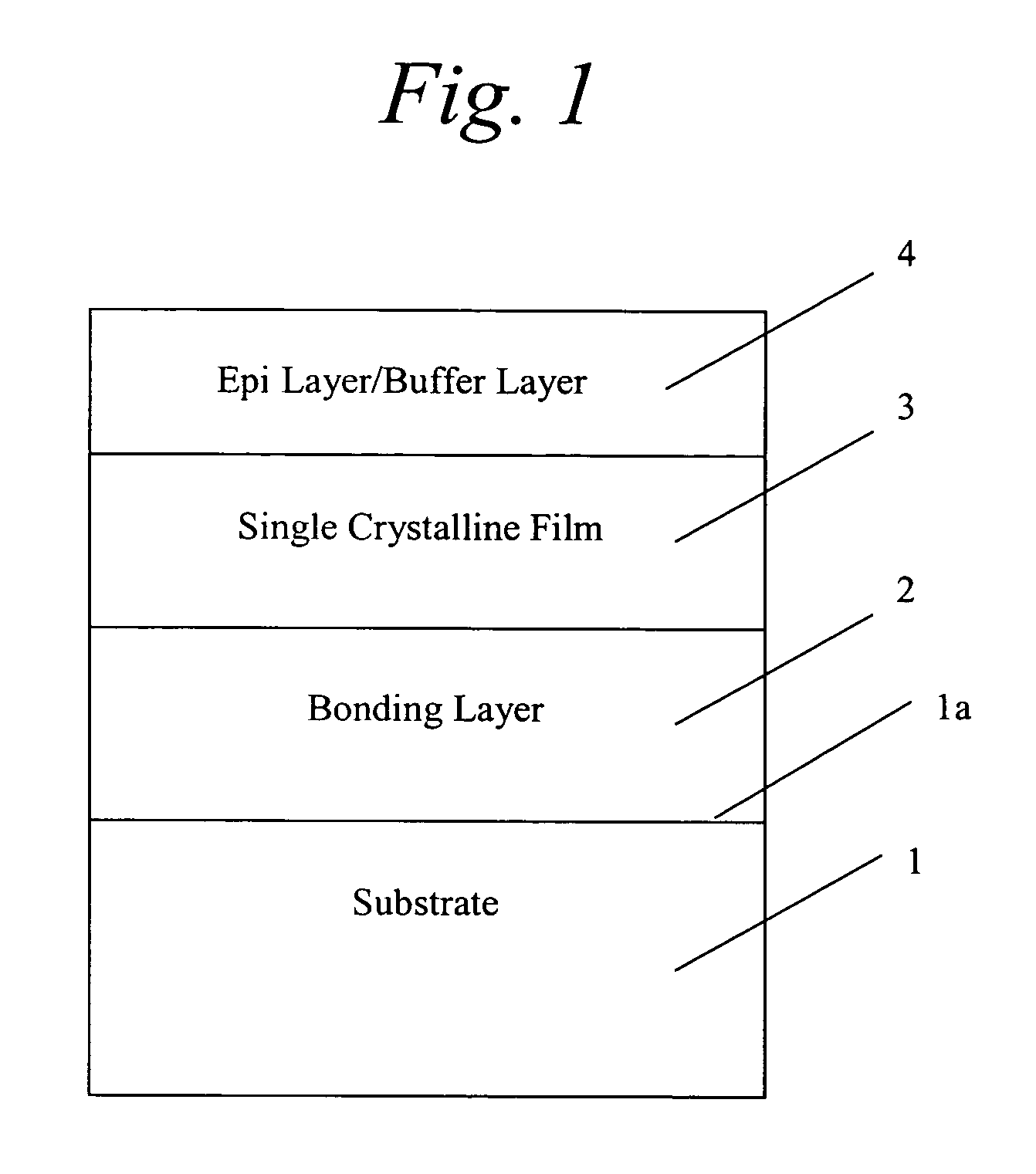
[0013] Accordingly, one aspect of the present invention produces a multi-layered substrate that su

Problems solved by technology

One of the main drawbacks to the production of these devices is the limited availability of suitable substrates for epitaxial growth.
However, the cost and availability of these wafers are prohibitive.
However, silicon does not have the thermal dissipation properties that are necessary for high power, high-speed devices.
In addition, Si and GaN have a significant thermal expansion mismatch.
However, this approach is inefficient and results in yield loss arising from the extra manufacturing steps required to manufacture two chips and wire them together.

Method used


Image

  • Novel method for integrating silicon CMOS and AlGaN/GaN wideband amplifiers on engineered substrates
  • Novel method for integrating silicon CMOS and AlGaN/GaN wideband amplifiers on engineered substrates
  • Novel method for integrating silicon CMOS and AlGaN/GaN wideband amplifiers on engineered substrates

Examples


examples

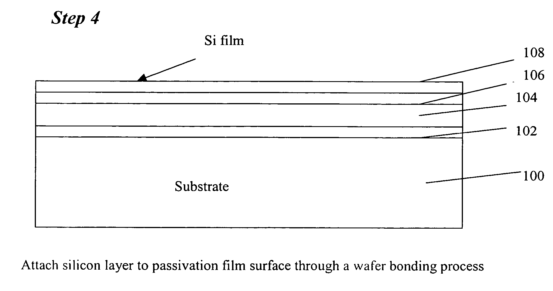
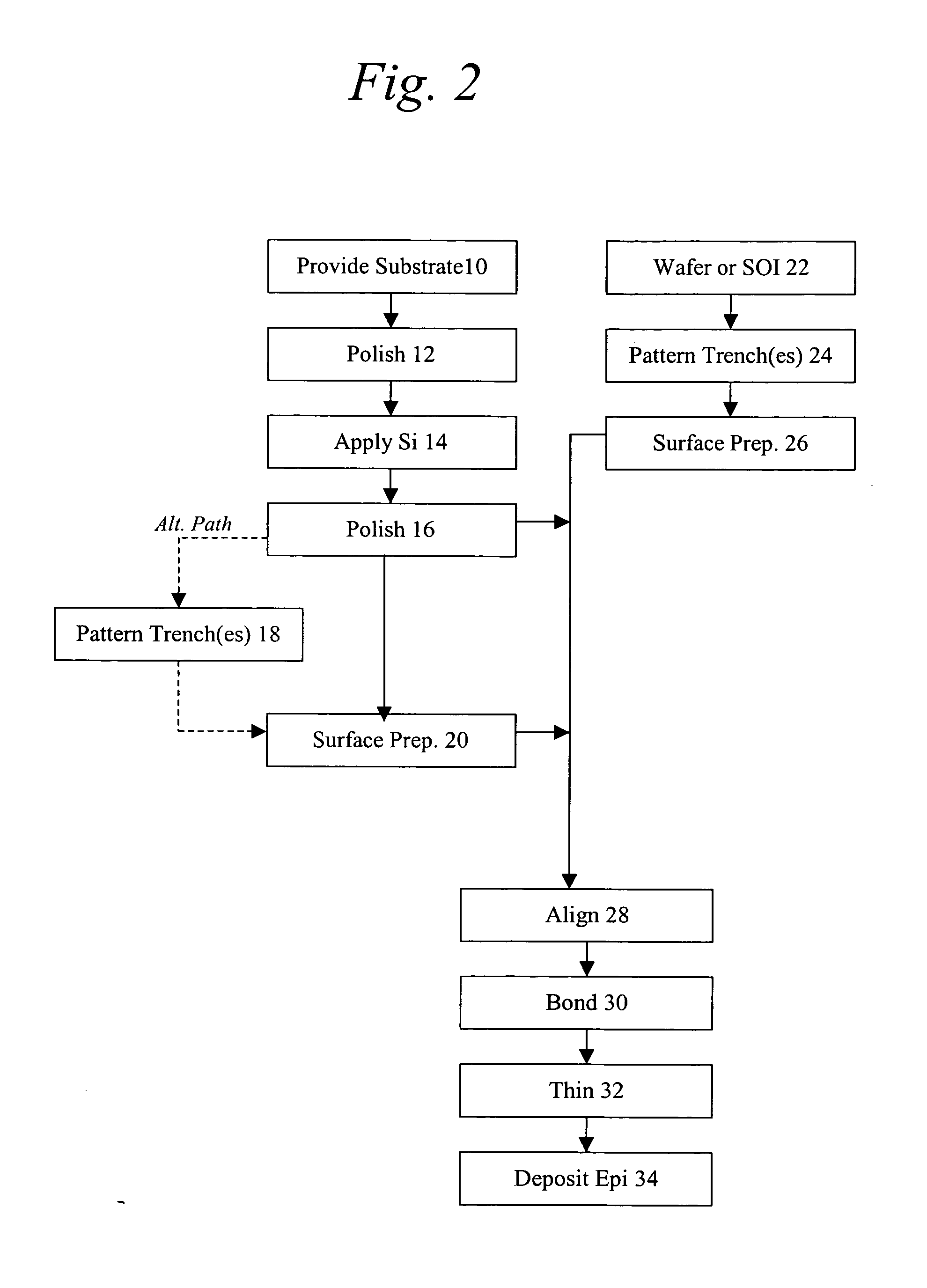
[0092] Two examples demonstrate the successful transfer of silicon to silicon carbide: (1) a silicon layer from a bulk silicon wafer to silicon carbide, and (2) a silicon layer from SOI to silicon carbide. Sonoscan images of the two are shown in FIGS. 16a and 16b. Bulk silicon, which is shown in FIG. 16a, was used for the first attempt in order to test the bonding process using the polished polycrystalline silicon carbide wafers. The center region shows small voids that can be attributed the planarization of the silicon layer. This particular set of wafers was thinned to approximately 100 μm.

[0093] The second example of bonding entailed bonding an SOI wafer to polycrystalline silicon carbide. The sonoscan in FIG. 16b shows a uniform bond without voids. This wafer was annealed at 175° C. and thinned to the buried oxide layer. FIG. 17 shows a cross-section of the wafer pair shown in FIG. 16b. In FIG. 17, several layers can be distinguished: the polycrystalline silicon carbide substra...


PUM


Abstract

High-speed silicon CMOS circuits and high-power AlGaN / GaN amplifiers are integrated on the same wafer. A thin layer of high resistivity silicon is bonded on a substrate. Following the bonding, an AlGaN / GaN structure is grown over the bonded silicon layer. A silicon nitride or a silicon oxide layer is then deposited over the AlGaN / GaN structure. Following this, a thin layer of silicon is bonded to the silicon nitride / silicon oxide layer. An area for the fabrication of AlGaN / GaN devices is defined, and the silicon is etched away from those areas. Following this, CMOS devices are fabricated on the silicon layer and AlGaN / GaN devices fabricated on the AlGaN / GaN surface.

Description

[0001] This application claims priority under 35 U.S.C. § 119 of provisional application No. 60 / 691,230, filed Jun. 17, 2005, the entire contents of which are hereby incorporated by reference.BACKGROUND OF THE INVENTION [0002] 1. Field of the Invention [0003] A CMOS transistor and an AlGaN / GaN amplifier are formed on the same substrate, where the substrate has high thermal efficiency. [0004] 2. Description of the Related Art [0005] Gallium nitride (GaN) is a wide-bandgap semiconductor material that has potential applications in high-speed, high power transistor devices. One of the main drawbacks to the production of these devices is the limited availability of suitable substrates for epitaxial growth. A high-quality bulk single crystal substrate at low cost that has a large area is desirable for the growth of gallium nitride epitaxial layers for device fabrication. In one example of the related art technology, the GaN epitaxial layer would be grown homoepitaxially on a single crysta...

Claims


Application Information

Patent Timeline
IPC IPC(8): H01L29/76H01L23/62
CPCH01L21/187H01L21/8258H01L29/2003H01L27/0605H01L27/1203H01L21/84
Inventor AUGUSTINE, GODFREYPARTLOW, DEBORAHTURLEY, ALFRED PAULKNIGHT, THOMASHARTMAN, JEFFREY D.
Owner NORTHROP GRUMMAN SYST CORP
Learn More