Flash memory and manufacturing method thereof

a technology of flash memory and manufacturing method, which is applied in the direction of semiconductor devices, basic electric elements, electrical apparatus, etc., can solve the problems of increasing processing difficulties, so-called critical dimension limitation of photolithographic process, and difficulty in reducing the line width of devices, so as to achieve simplified processing steps and reduce production costs

Active Publication Date: 2006-12-07
POWERCHIP SEMICON MFG CORP
View PDF5 Cites 4 Cited by
  • Summary
  • Abstract
  • Description
  • Claims
  • Application Information

AI Technical Summary

Benefits of technology

[0010] Accordingly, at least one objective of the present invention is to provide a flash memory and method of manufacturing the same that utilizes a self-aligned process to form a floating gate and a select gate. Hence, the processing steps are simplified and the production cost is reduced.
[0011] At least a second objective of the present invention is to provide a flash memory and manufacturing method thereof that can increase the gate-coupling ratio between the floating gate and the control gate, improve the performance of the device, and increase the product yield.

Problems solved by technology

However, defining the floating gate and the control gate through the photolithographic and etching processes not only increases processing difficulties, but also leads to the so-called critical dimension limitation of the photolithographic process.
Consequently, it is very difficult to reduce the line width of devices, thereby creating an immense barrier for increasing the level of integration of the devices.

Method used


Image

  • Flash memory and manufacturing method thereof
  • Flash memory and manufacturing method thereof
  • Flash memory and manufacturing method thereof

Examples


Embodiment Construction

[0043] Reference will now be made in detail to the present preferred embodiments of the invention, examples of which are illustrated in the accompanying drawings. Wherever possible, the same reference numbers are used in the drawings and the description to refer to the same or like parts.

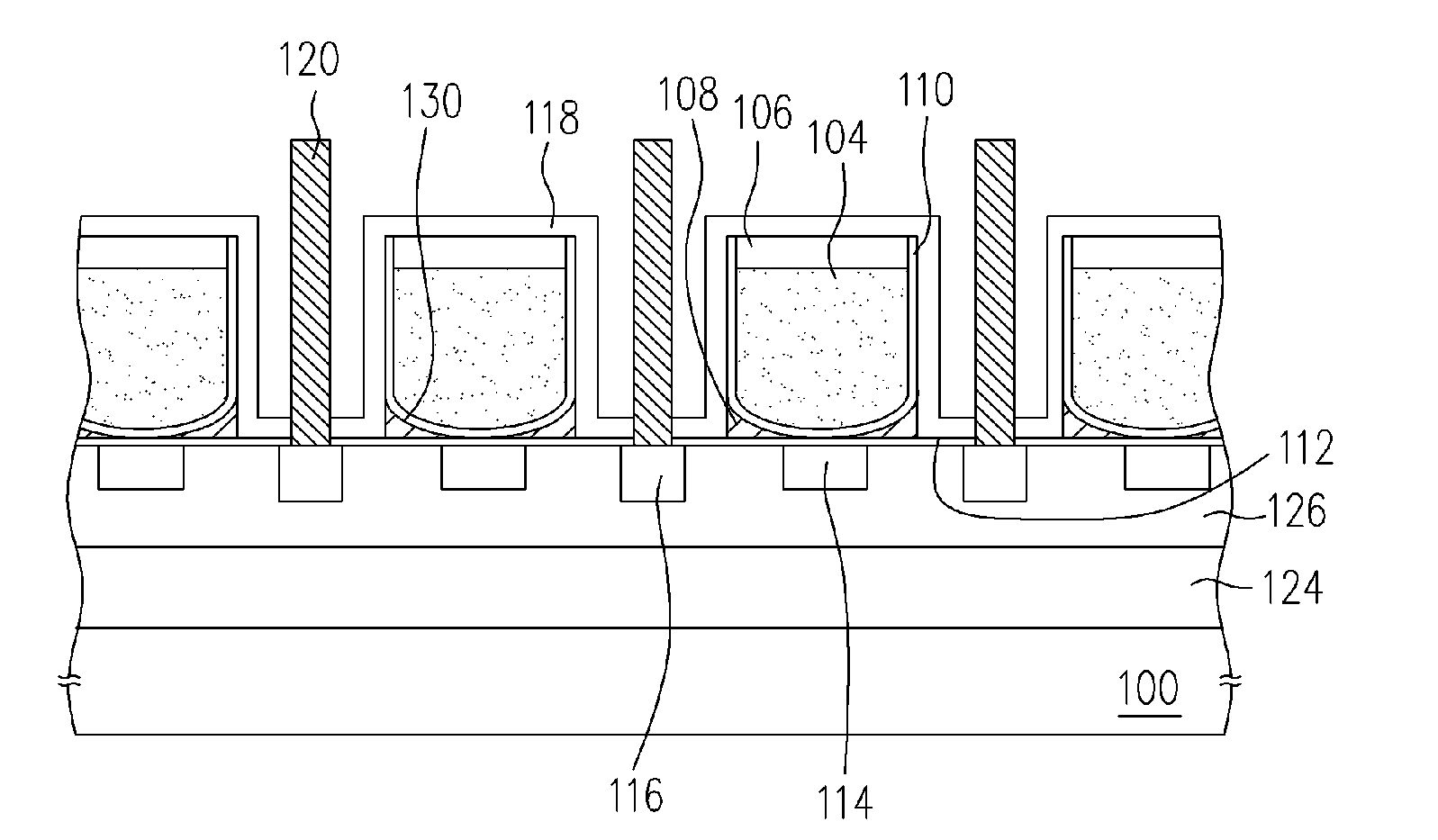
[0044]FIG. 1A is a top view of a flash memory according to one preferred embodiment of the present invention. FIG. 1B is a cross-sectional view along line A-A′ of FIG. 1A. As shown in FIGS. 1A and 1B, the flash memory mainly includes a substrate 100, a plurality of device isolation structures 102, a plurality of control gates 104, a plurality of cap layers 106, a plurality of floating gates 108, a plurality of inter-gate dielectric layers 110, a plurality of tunneling dielectric layers 112, a plurality of doped regions 114, a plurality of source / drain regions 116, an insulating layer 118 and a plurality of conductive plugs 120.

[0045] The substrate 100 is a silicon substrate with a deep N-well 124 ...


PUM


Abstract

A method for manufacturing flash memory is provided. A tunneling dielectric layer, a conductive layer and a patterned mask layer that exposes a portion of the conductive layer are formed on a substrate. An oxide layer is formed on the exposed conductive layer so that the conductive layer is partitioned through the oxide layer into blocks. The oxide layer is removed and an inter-gate dielectric layer is formed in the opening. A control gate that completely fills the opening is formed. A cap layer is formed over the control gate. The mask layer is then removed. Using the cap layer as a mask, a portion of the conductive layer is removed to form two floating gates under the control gate. An insulating layer is formed on the substrate. Source / drain regions are formed in the substrate on the respective sides of the control gate.

Description

CROSS-REFERENCE TO RELATED APPLICATION [0001] This application claims the priority benefit of Taiwan application serial no. 94118692, filed on Jun. 07, 2005. All disclosure of the Taiwan application is incorporated herein by reference. BACKGROUND OF THE INVENTION [0002] 1. Field of the Invention [0003] The present invention relates to a semiconductor device. More particularly, the present invention relates to a flash memory and manufacturing method thereof. [0004] 2. Description of the Related Art [0005] Memory is a type of semiconductor device for holding information and storing digital data. As the microprocessor of a computer becomes more powerful, the size of software programs and the amount of computation that can be carried out increase exponentially. As a result, the demand for memory with very high storage capacity increases at an alarming rate. To fabricate memories with a large storage at a low production cost, techniques and processes that can increase the level of integr...

Claims


Application Information

Patent Timeline
Patent Type & Authority Applications(United States)
IPC IPC(8): H01L21/336
CPCH01L21/28273H01L27/115H01L29/7887H01L29/42324H01L27/11521H01L29/40114H10B69/00H10B41/30
Inventor CHUANG, I-CHUNHSU, CHENG-YUANPAN, JUI-YU
Owner POWERCHIP SEMICON MFG CORP
Why Eureka
Try Eureka