Self light-emitting device
a self-lighting and light-emitting technology, applied in the direction of discharge tube luminescnet screens, non-linear optics, instruments, etc., can solve the problems of reducing the luminescence efficiency of the outside of the light-emitting element, reducing the efficiency of extraction of light, and generating solid-state light, so as to improve the state of interface, improve the efficiency of extracting light generated in the light-emitting layer, and improve the effect of luminescence efficiency
- Summary
- Abstract
- Description
- Claims
- Application Information
AI Technical Summary
Benefits of technology
Problems solved by technology
Method used
Image

Examples
embodiment 1
[0023]FIG. 4 is a diagram showing the cross sectional structure of an active matrix type self light-emitting device of the present invention. In FIG. 4, reference numeral 401 denotes a substrate and 402 denotes a TFT. It is to be noted that a known TFT is used as the TFT 402. Furthermore, reference numeral 403 denotes an electrode having aluminum (AL) as its principal constituent, and a polyparaphenylene vinylene (PPV) is used for an EL layer 404. Reference numeral 405 denotes a transparent electrode made of ITO, and argon is filled in a gas space denoted by 406. Also, glass is used as a cover material 407 and spacers 408 are utilized in the gas space 406 to secure it.
embodiment 2
[0024]FIG. 5 is a diagram showing a cross sectional structure of a passive matrix type self light-emitting device of the present invention. In FIG. 5, reference numeral 501 denotes a substrate and 502 denotes an EL layer. PPV is used for the EL layer. Reference numeral 503 denotes a plurality of opaque electrodes (cathodes) arranged in stripe shapes and a plurality of transparent electrodes (anodes) 504 are provided in stripe shapes so as to be orthogonal to the plurality of opaque electrodes 503.
[0025] In addition, the EL layer 502 is formed sandwiched between the plurality of opaque electrodes 503 and the plurality of transparent electrodes 504. At this point, a cover material 506 made of glass is provided on the plurality of transparent electrodes 504, sandwiching spacers 507. A gas space 505 is thus formed between the cover material 506 and the plurality of electrodes 504. Nitrogen is filled in the gas space 505 in Embodiment 2. Note that the constitution of Embodiment 2 may be...
embodiment 3
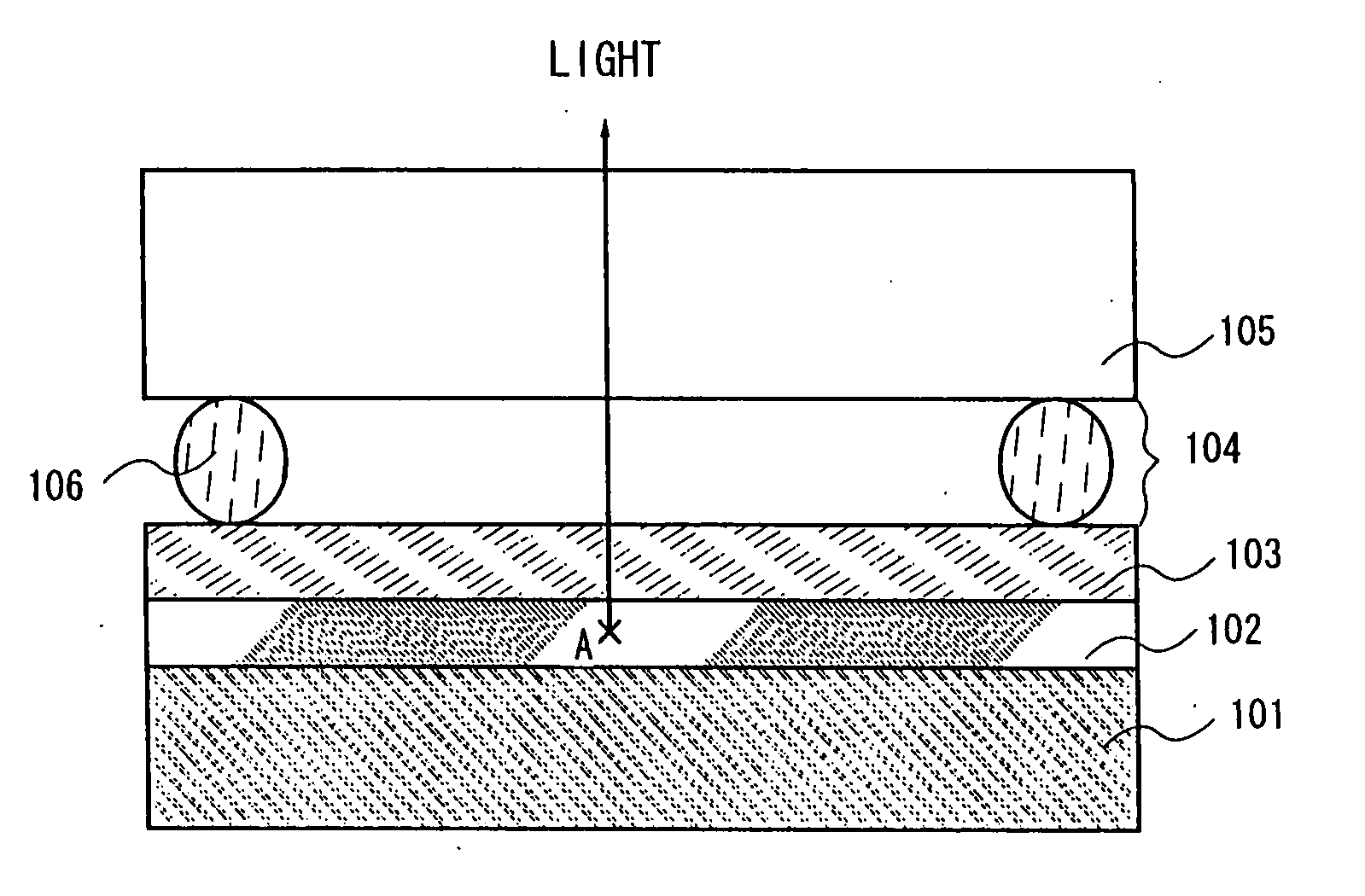
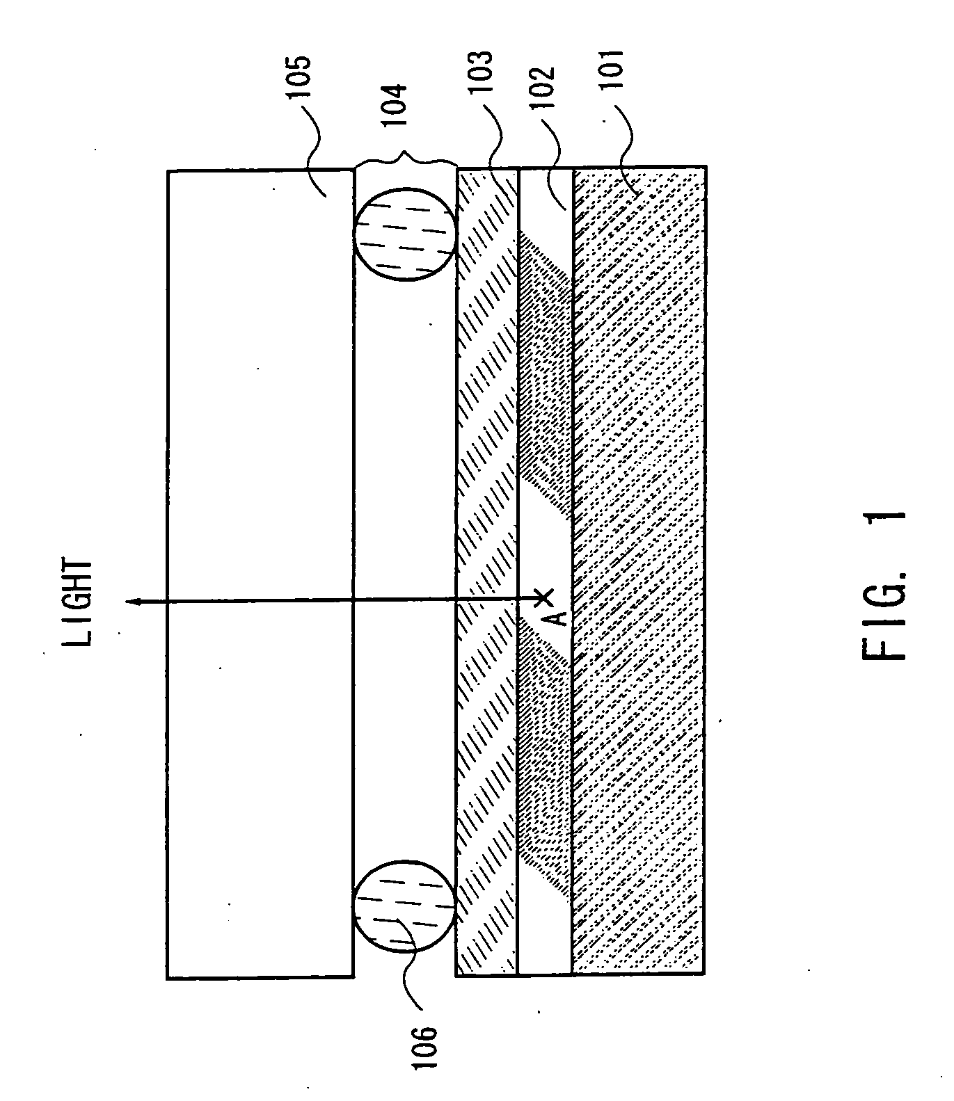
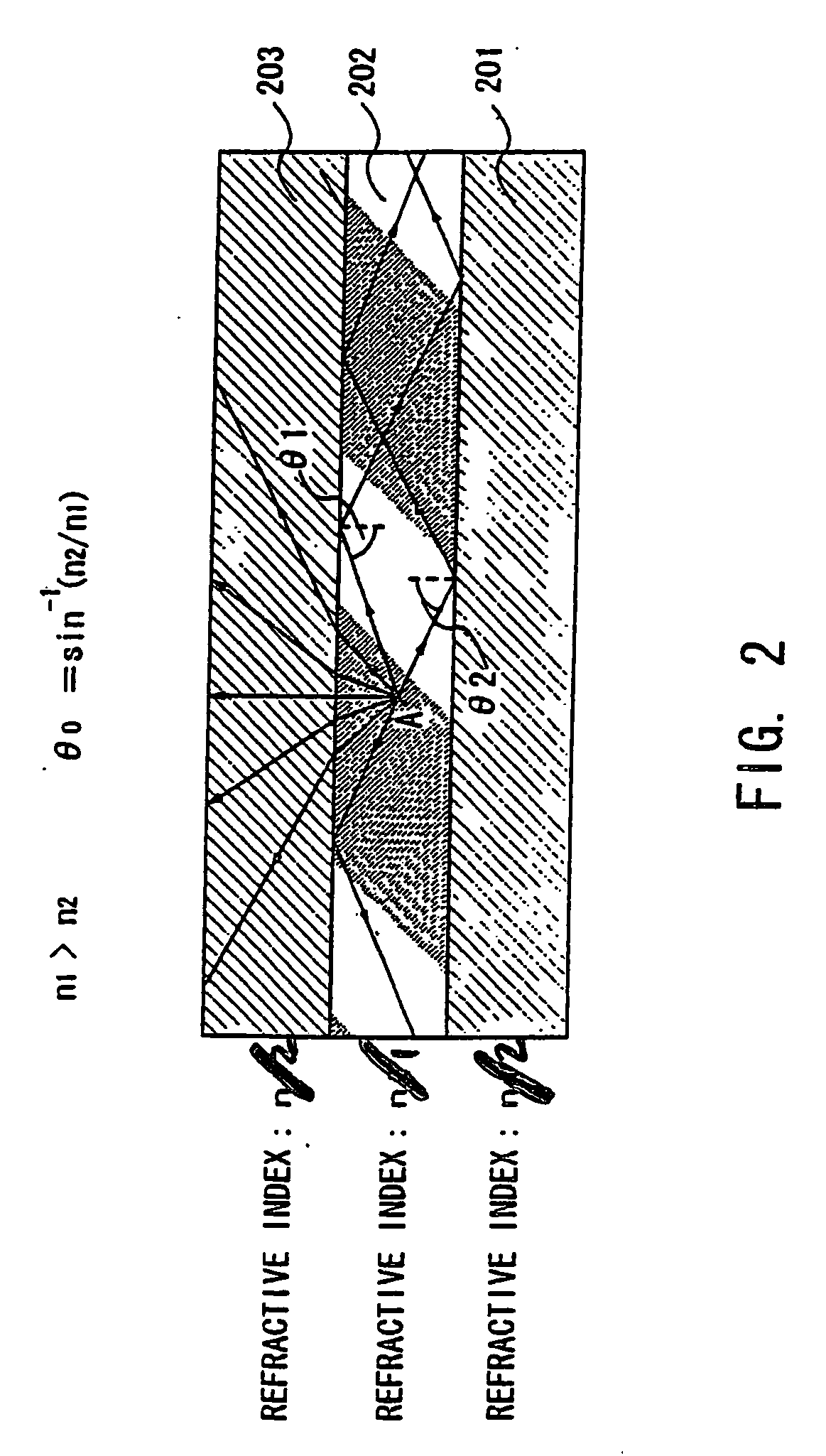
[0026] As shown in FIG. 3, the EL layer 305 comprises the light-emitting layer 303 and, as buffer layers, the electron injection layer 302 and the hole injection layer 304. A polymer-based material is used for the layers constituting the El layer 305. For example, polyparaphenylene vinylene can be used for the light-emitting layer 303, copper pthalocyanine or PEDOT for the buffer layer (hole injection layer) 304, and lithium fluoride or lithium for the buffer layer (electron injection layer) 302.
[0027] Note that in forming the EL layer 305, it is desirable that the treatment atmosphere for conducting the formation of this layer is a dry atmosphere having as little moisture as possible and in inert gas. The inert gas here is one such as nitrogen or argon. Because the EL layer easily deteriorates due to the presence of moisture or oxygen, it is therefore necessary to eliminate these factors as much as possible when forming this layer. In addition, these layers which constitute the EL...
PUM
 Abstract
Description
Claims
Application Information
 - R&D
- Intellectual Property
- Life Sciences
- Materials
- Tech Scout
- Unparalleled Data Quality
- Higher Quality Content
- 60% Fewer Hallucinations
Browse by: Latest US Patents, China's latest patents, Technical Efficacy Thesaurus, Application Domain, Technology Topic, Popular Technical Reports.
© 2025 PatSnap. All rights reserved.Legal|Privacy policy|Modern Slavery Act Transparency Statement|Sitemap|About US| Contact US: help@patsnap.com