Method and system for the directional detection of electrons in a scanning electron microscope
a scanning electron microscope and electron directional detection technology, applied in the field of scanning electron microscope system for directional detection of electrons, can solve the problem of complex detection system of secondary electrons
- Summary
- Abstract
- Description
- Claims
- Application Information
AI Technical Summary
Benefits of technology
Problems solved by technology
Method used
Image
Examples
first embodiment
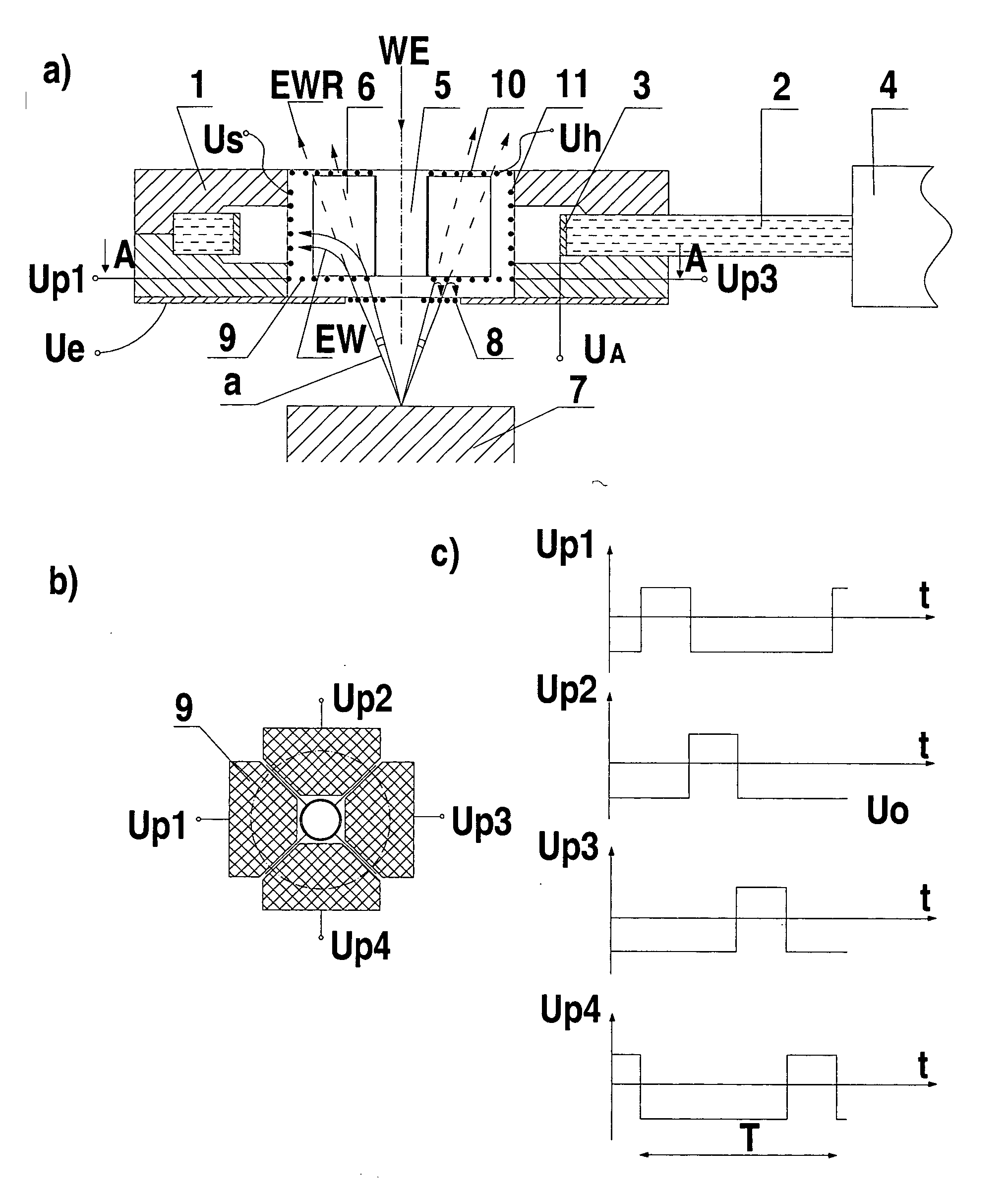
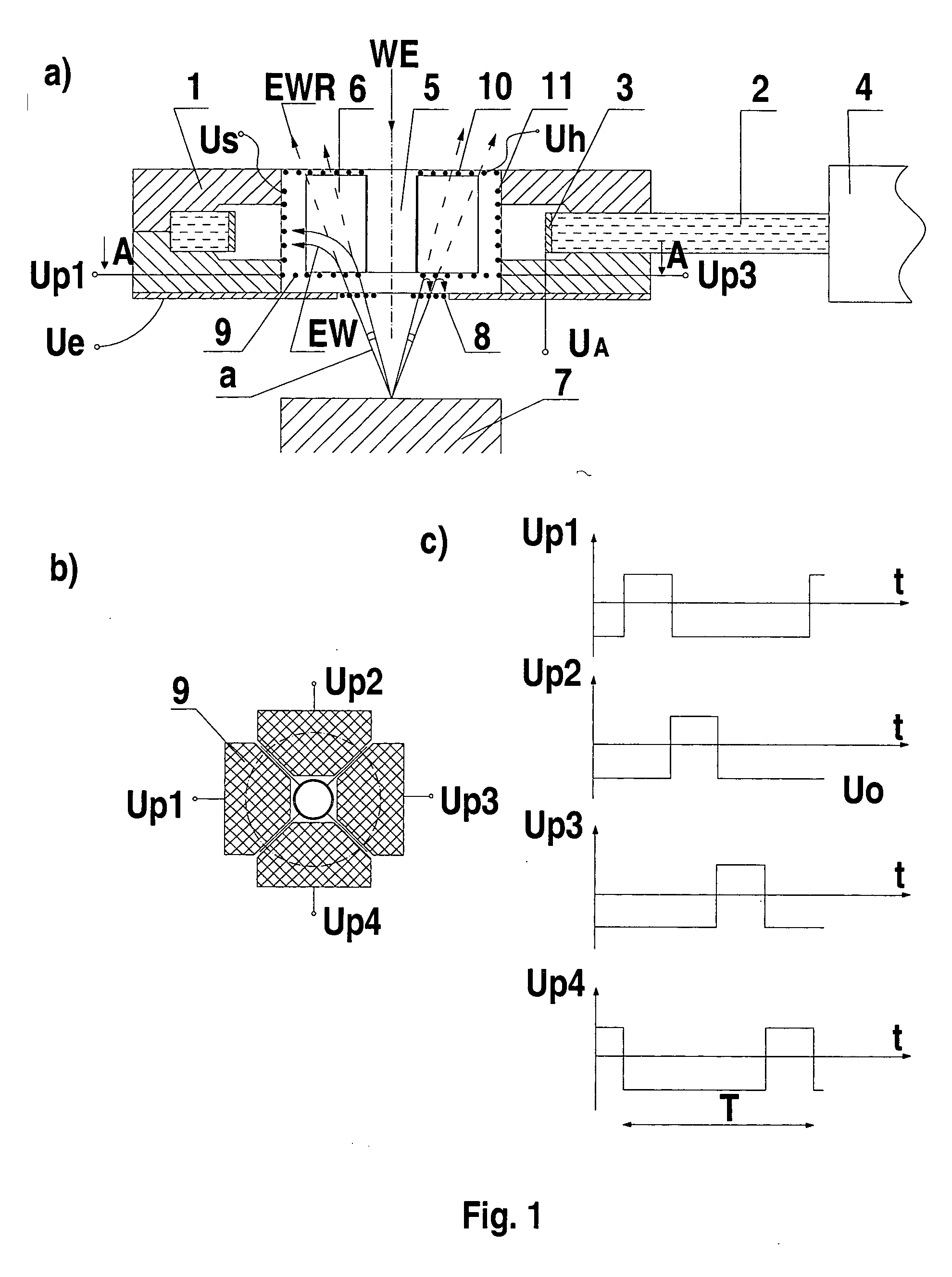
[0026] the invention will now be described with reference to FIGS. 1a to 1c.
[0027] The system for a directional detection of electrons in a scanning electron microscope shown in FIG. 1a is mounted in a ring-shaped head body 1 made of teflon. A light conductor or light pipe 2 is located in a slot of the two-piece head body 1 and is in the form of a plexiglass plate with an opening covered with a scintillator 3 on its perimeter. The light pipe 2 is connected to a photomultiplier 4. Inside the head body 1, a screen pipe 5 is located with four screen plates 6 attached symmetrically which divide a hole in the head body 1 into four sectors. In a lower part of the head body 1, on a side of the head body facing toward a sample stage 7, an input grid 8 is located. Above the input grid 8, four sector electron flow control electrodes 9 are located and each one is placed in one sector formed between the screen plates 6. The sector flow control electrodes 9 each are made of a metal grid. A reta...
second embodiment
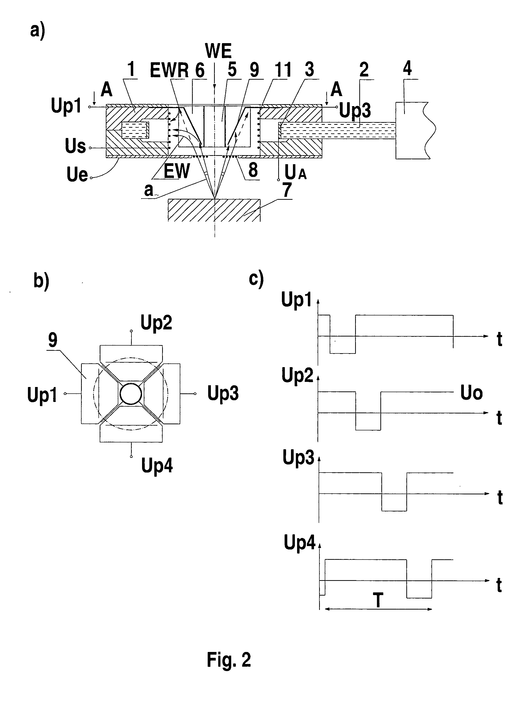
[0030] the invention will now be described with reference to FIGS. 2a to 2c.
[0031] The system for the directional detection of electrons in a scanning electron microscope shown in FIG. 2a is designed similarly to the first embodiment and is mounted in a ring-shaped head body 1 made of teflon. A light conductor or light pipe 2 is located in a slot of the two-piece head body 1 and is in the form of a plexiglass plate with a hole covered with a scintillator 3 on its perimeter. The light pipe 2 is connected to a photomultiplier 4. A screen pipe 5 with four screen plates 6 divides the hole in the head body 1 interior into four sectors. An input grid 8 is located in a lower part of the head body 1 on a side of the head body facing toward a sample stage 7. Electron flow control electrodes 9 are located above the input grid 8 in the upper part of the head body 1 with each one of the electron flow control electrodes being placed in one sector formed between the screen plates 6. The sector f...
third embodiment
[0035] the invention will now be described with reference to FIGS. 3a to 3d.
[0036] The system for the directional detection of electrons in a scanning electron microscope shown in FIG. 3a is adapted to operate in a low vacuum scanning electron microscope. The unit is mounted in a head body 1, made of teflon. A lower throttling aperture 12 is located in the lower part of the head body 1 facing toward a sample stage 7 and formed as a metal plate with a small hole. The hole is coaxial with the axis of the primary electron beam WE. A microporous plate 13 is located above the lower throttling aperture 12. The microporous plate 13 has a hole also coaxial with the axis of the primary electron beam WE. Inside the mircroporous plate 13, a screening pipe 5 is fixed by means of a teflon seal. A lower entrance surface of the microporous plate 13 which faces toward the sample stage is coated with a thin conducting layer, permeable for electrons. A similar thin conducting layer is also present o...
PUM
 Abstract
Description
Claims
Application Information
 - R&D
- Intellectual Property
- Life Sciences
- Materials
- Tech Scout
- Unparalleled Data Quality
- Higher Quality Content
- 60% Fewer Hallucinations
Browse by: Latest US Patents, China's latest patents, Technical Efficacy Thesaurus, Application Domain, Technology Topic, Popular Technical Reports.
© 2025 PatSnap. All rights reserved.Legal|Privacy policy|Modern Slavery Act Transparency Statement|Sitemap|About US| Contact US: help@patsnap.com


