
Flexible PCB having surplus bends for electronic equipment

a technology of electronic equipment and surplus bends, applied in the field of flexible pcb, can solve the problems of severing wires, more serious bending fatigue of flexible pcb,

Inactive Publication Date: 2006-09-28
SAMSUNG ELECTRO MECHANICS CO LTD
View PDF4 Cites 26 Cited by
  • Summary
  • Abstract
  • Description
  • Claims
  • Application Information

AI Technical Summary

Benefits of technology

[0017] Accordingly, the present invention has been made keeping in mind the above problems occurring in the prior art, and an object of the present invention is to provide a flexible PCB which can be used as an connection between two rigid PCBs that move relative to each other, for a long period of time without causing wires formed therein to be severed by the bending fatigue accumulated due to the relative movement.
[0018] Another object of the present invention is to provide a flexible PCB which has excellent durability against bending fatigue and can improve the quality of the electronic appliance, such as mobile phones, digital cameras, camcorders, etc., to which it is applied.

Problems solved by technology

In a mobile phone of the composite structure, the flexible PCB experiences more serious bending fatigue because the relative movement (swinging on a hinge) between a display part having an LCD panel, and a main body having a keypad occurs more frequently and the swinging range is larger.
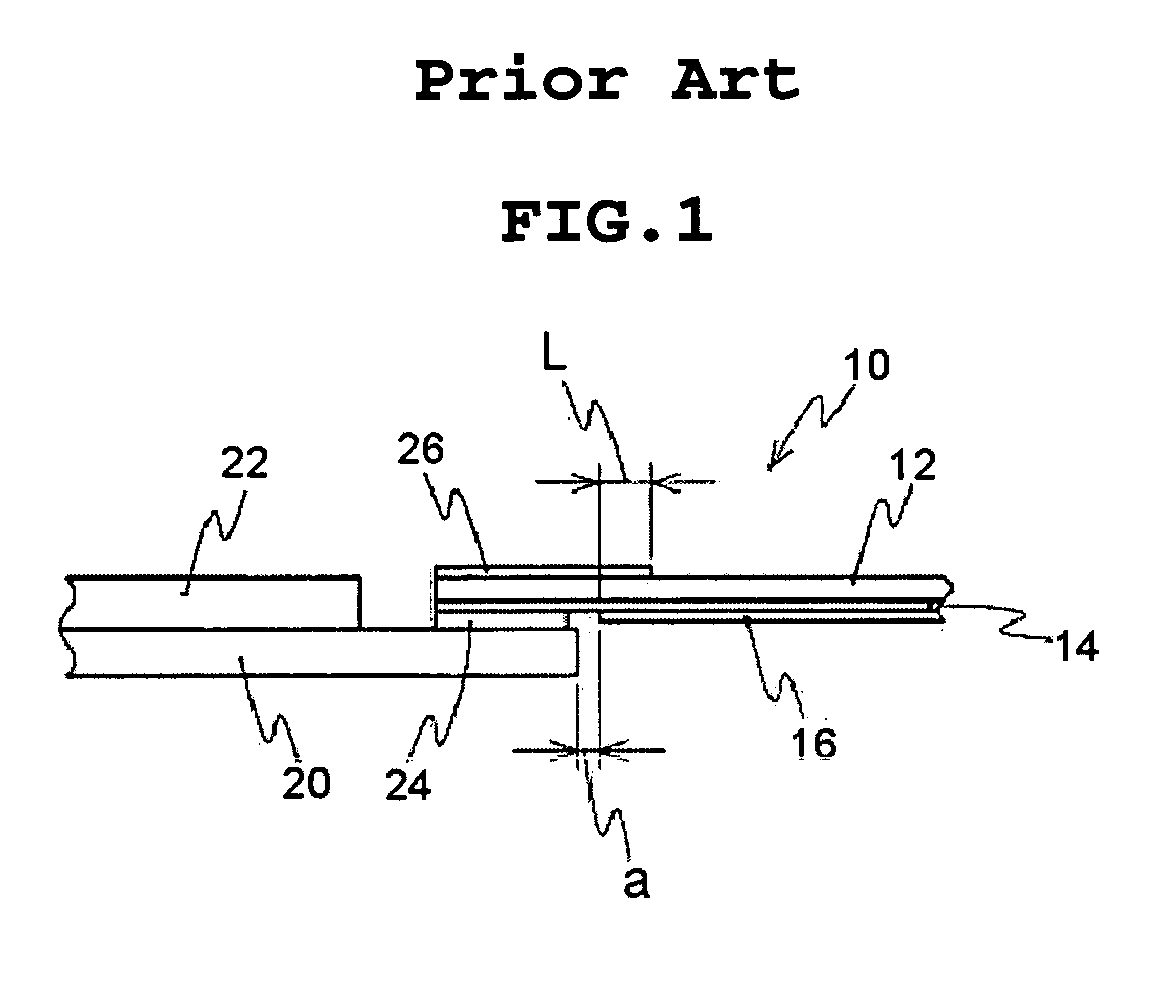
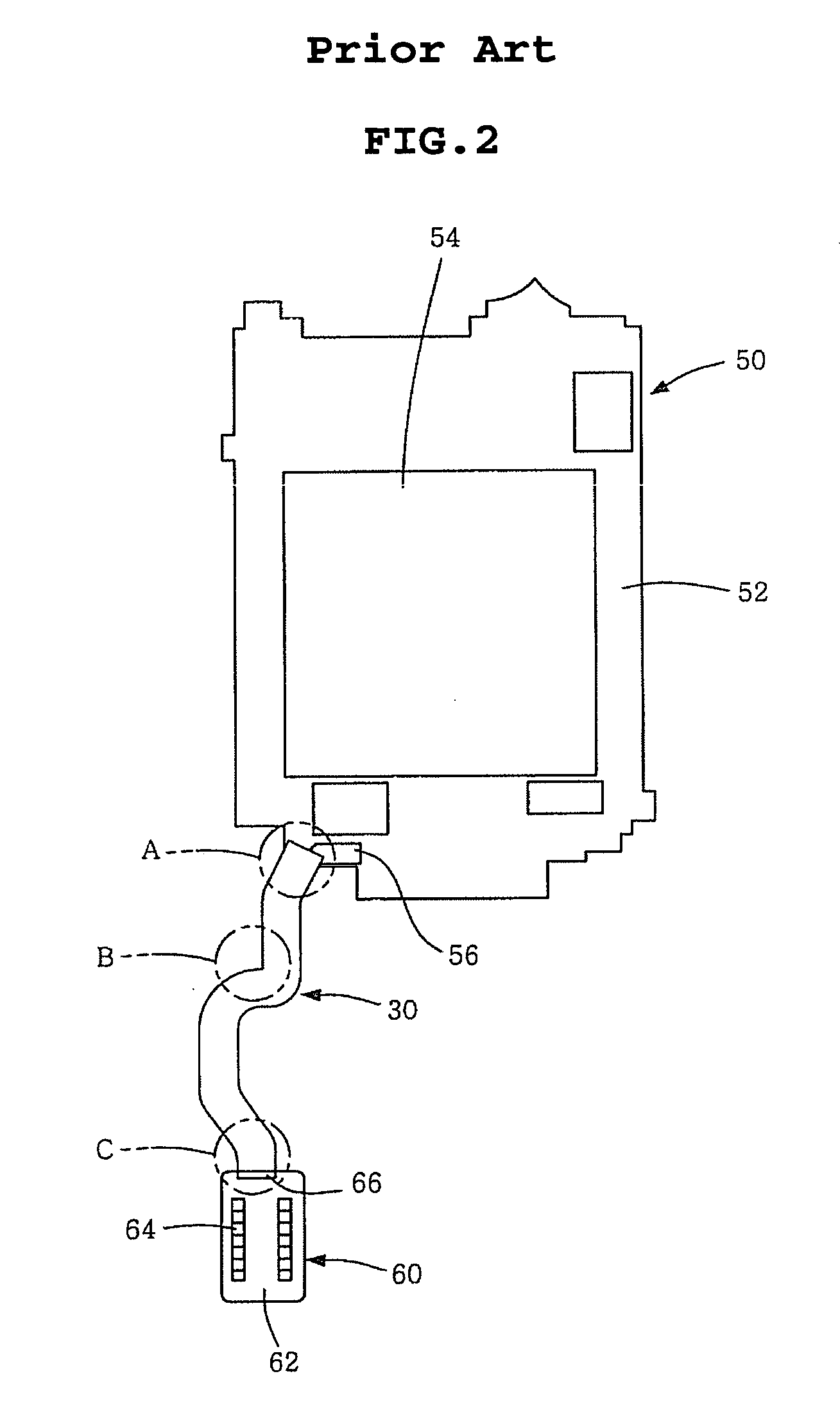
For example, a flexible PCB employed in a folding-type mobile phone, as shown in FIG. 2, may have stress concentrated on the opposite ends thereof and at its parts which are in contact with other structures, thereby undergoing a severing of wires due to the resultant bending fatigue.

Method used


Image

  • Flexible PCB having surplus bends for electronic equipment
  • Flexible PCB having surplus bends for electronic equipment
  • Flexible PCB having surplus bends for electronic equipment

Examples


Embodiment Construction

[0033] Reference now should be made to the drawings, in which the same reference numerals are used throughout the different drawings to designate the same or similar components.

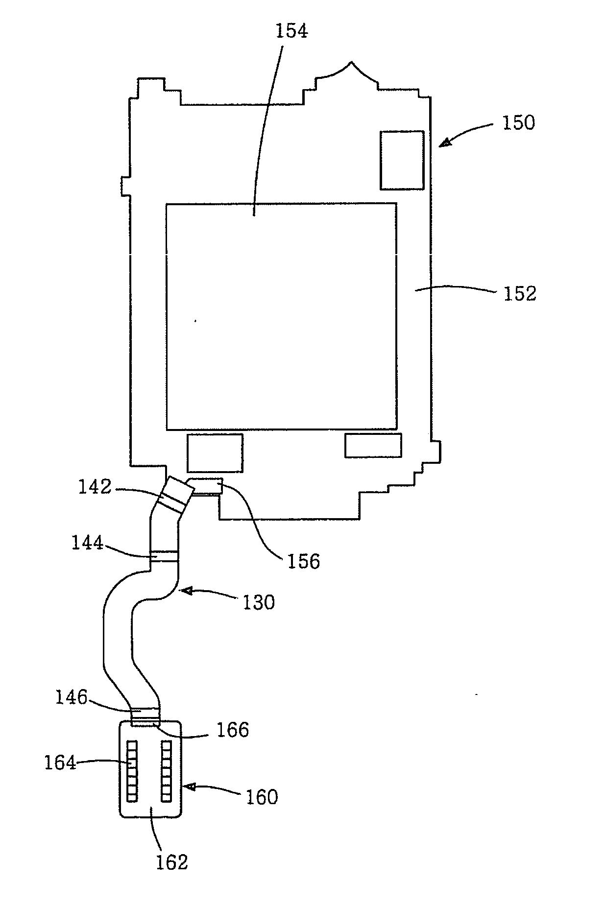
[0034] In FIGS. 3 to 5, a flexible PCB in accordance with one embodiment of the present invention and a folding-type mobile phone to which the flexible PCB is applied are shown. FIG. 3 is a schematic partial view of the folding-type mobile phone, FIG. 4 shows the flexible substrate of FIG. 3 in a perspective view, and FIG. 5 is an assembled perspective view of the folding-type mobile phone, with a partially enlarged hinge portion insetted.

[0035] As shown in FIGS. 3 and 4, a flexible PCB 130 according to the present invention acts as a bridge between a first PCB 150 mounted in a structure, such as a display part of the folding-type mobile phone, and a second PCB 160 mounted in a structure, such as a main body (not shown) of the folding-type mobile phone. The first PCB 150 includes a window 154 for installing...


PUM


Abstract

A flexible PCB is provided with surplus bends so that it can be readily bent according to the repetitive movement thereof, whereby wires formed in the flexible PCB can be prevented from being severed by the bending fatigue accumulated due to the movement. The flexible PCB for use in electronic equipment acts to transmit electrical signals between two rigid PCBs and acts as a structural bridge therebetween, the two rigid PCBs being spaced away from each other and being able to relatively move. The flexible PCB includes: a plurality of wires, each functioning as a passageway for electrical signals; and a soft material-based substrate body in which the wires are formed; and being provided with surplus bends at predetermined positions so as to allow the flexible PCB to resiliently move according to the relative movement of the rigid PCBs.

Description

INCORPORATION BY REFERENCE [0001] The present application claims priority under 35 U.S.C. §119 to Korean Patent Application No. 10-2005-0025245 filed on Mar. 26, 2005. The content of the application is incorporated herein by reference in its entirety. BACKGROUND OF THE INVENTION [0002] 1. Field of the Invention [0003] The present invention relates generally to a flexible PCB for use in electronic equipment. More particularly, the present invention relates to a flexible PCB which is provided with surplus bends so that it can be readily bent according to the repetitive movement thereof, whereby wires formed in the flexible PCB can prevented from being severed by the bending fatigue accumulated due to the movement. [0004] 2. Description of the Related Art [0005] With the ability to be readily bent, flexible printed circuit boards (PCBs), most of which are manufactured by patterning copper conductors on polyimide films, are used in electronic equipment, such as printers, mobile phones, ...

Claims


Application Information

Patent Timeline
Patent Type & Authority Applications(United States)
IPC IPC(8): H05K1/03
CPCH05K1/028H05K1/148H05K2201/091H05K1/02
Inventor MOON, YANG HOOH, SE MIN
Owner SAMSUNG ELECTRO MECHANICS CO LTD
Learn More