Method of manufacturing EL panel
- Summary
- Abstract
- Description
- Claims
- Application Information
AI Technical Summary
Benefits of technology
Problems solved by technology
Method used
Image
Examples
example 1
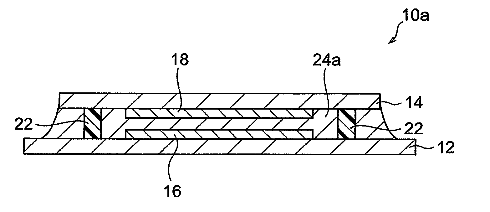
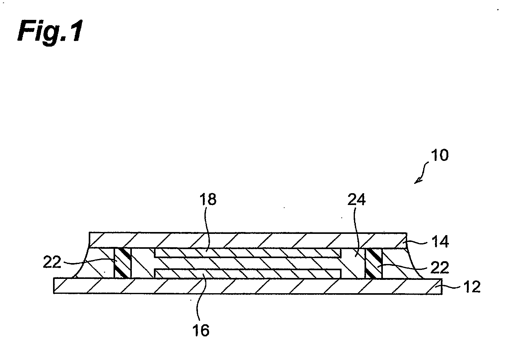
[0057] First, an organic EL device in which an EL device portion was provided on a substrate was formed. Next, a spacer portion comprising a resin was disposed around the perimeter of the EL device portion on the substrate, and then a UV cationic curing type epoxy resin (XNR5570, made by Nagase Chemtex Corporation) was dripped as a sealant onto the region surrounded by the spacer. A transparent sealing plate having a color filter portion provided thereon was then disposed on the substrate such that the EL device portion and the color filter portion faced one another, and the substrate and the sealing plate were bonded together by applying pressure thereto, whereby a panel precursor was obtained.
[0058] After that, the panel precursor obtained was irradiated from the sealing plate side with UV light (output 13,000 mJ / cm2) emitted from a high-pressure mercury lamp. The sealant was thus irradiated with UV light attenuated by the color filter portion. The UV cationic curing type epoxy r...
PUM
 Abstract
Description
Claims
Application Information
 - R&D
- Intellectual Property
- Life Sciences
- Materials
- Tech Scout
- Unparalleled Data Quality
- Higher Quality Content
- 60% Fewer Hallucinations
Browse by: Latest US Patents, China's latest patents, Technical Efficacy Thesaurus, Application Domain, Technology Topic, Popular Technical Reports.
© 2025 PatSnap. All rights reserved.Legal|Privacy policy|Modern Slavery Act Transparency Statement|Sitemap|About US| Contact US: help@patsnap.com


