
Semiconductor fabrication processes

a technology of semiconductors and fabrication processes, applied in the direction of electrical equipment, basic electric elements, capacitors, etc., can solve the problems of increasing the problem of non-selectivity of etching, lack of suitably selective etching chemistry having a sufficiently high etching rate to perform in high aspect ratio features

Inactive Publication Date: 2006-08-10
MICRON TECH INC
View PDF21 Cites 28 Cited by
  • Summary
  • Abstract
  • Description
  • Claims
  • Application Information

AI Technical Summary

Benefits of technology

The invention provides several chemistries that can be used to selectively etch metal-containing materials, such as metal nitride, relative to silicon, silicon dioxide, silicon nitride, and doped silicon oxide. One chemistry involves a mixture of hydrogen peroxide and ammonium hydroxide or tetra-methyl ammonium hydroxide. Another chemistry involves a mixture of hydrogen peroxide and hydrochloric acid. Other chemistries involve the use of persulfate, ozone, or phosphate. These chemistries can be used to selectively etch metal nitride and related materials, which can be useful in various semiconductor manufacturing processes.

Problems solved by technology

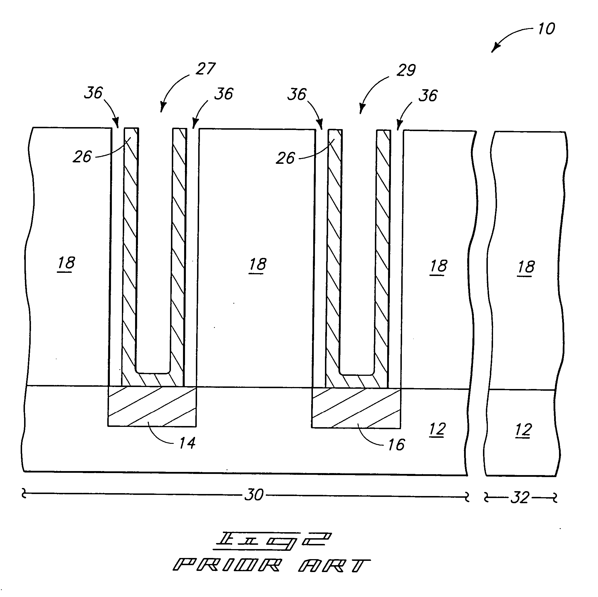
The non-selectivity of the etch becomes increasingly problematic as an aspect ratio of openings 36 increases.
Such is a problem with conventional etching processes.
A difficulty in conducting the above-described prior art processing occurs during removal of material 24 (FIG. 1), and results from a lack of a suitably selective etch chemistry having a sufficiently high etch rate to perform in high aspect ratio features.

Method used


Image

  • Semiconductor fabrication processes
  • Semiconductor fabrication processes
  • Semiconductor fabrication processes

Examples


example 1

[0056] An etching solution is formed by mixing 400 parts of hydrogen peroxide with 5 parts of ammonium hydroxide. The hydrogen peroxide is 30 weight percent in water and the ammonium hydroxide is 29 weight percent in water. Accordingly, the final solution comprises approximately 30 weight percent hydrogen peroxide, 0.36 weight percent ammonium hydroxide, and 70 weight percent water.

example 2

[0057] An etching solution is formed by mixing 400 parts of hydrogen peroxide with 5 parts of tetra-methyl ammonium hydroxide. The hydrogen peroxide is 30 weight percent in water and the tetra-methyl ammonium hydroxide is 25 weight percent in water. Accordingly, the etching solution comprises 30 weight percent hydrogen peroxide, 0.31 weight percent tetra-methyl ammonium hydroxide, and 70 weight percent water.

example 3

[0058] An etching solution is formed by mixing 400 parts of hydrogen peroxide with 20 parts of hydrochloric acid. The hydrogen peroxide is 30 weight percent in water and the hydrochloric acid is 35 weight percent in water. Accordingly, the etching solution comprises about 29% hydrogen peroxide, 1.7% hydrochloric acid, and 69% water.


PUM


Abstract

Various methods for selectively etching metal-containing materials (such as, for example, metal nitrides, which can include, for example, titanium nitride) relative to one or more of silicon, silicon dioxide, silicon nitride, and doped silicon oxides in high aspect ratio structures with high etch rates. The etching can utilize hydrogen peroxide in combination with ozone, ammonium hydroxide, tetra-methyl ammonium hydroxide, hydrochloric acid and / or a persulfate. The invention can also utilize ozone in combination with hydrogen peroxide, and / or in combination with one or more of ammonium hydroxide, tetra-methyl ammonium hydroxide and a persulfate. The invention can also utilize ozone, hydrogen peroxide and HCl, with or without persulfate. The invention can also utilize hydrogen peroxide and a phosphate, either alone, or in combination with a persulfate.

Description

TECHNICAL FIELD [0001] The invention pertains to methods of removing metal-containing materials, and in particular aspects pertains to methods suitable for incorporation into semiconductor fabrication processes during formation of capacitor constructions. BACKGROUND OF THE INVENTION [0002] Numerous applications exist in which it is desired to selectively etch metal-containing materials relative to other materials. One such application is fabrication of capacitor structures during semiconductor processing. An exemplary process for forming capacitor structures is described with reference to FIGS. 1-4. [0003] Referring initially to FIG. 1, a semiconductor wafer fragment 10 is illustrated at a preliminary processing stage. Fragment 10 comprises a substrate 12 supporting a pair of conductive nodes 14 and 16. [0004] Substrate 12 can comprise, for example, monocrystalline silicon lightly doped with background p-type dopant. To aid in interpretation of the claims that follow, the terms “sem...

Claims


Application Information

Patent Timeline
Patent Type & Authority Applications(United States)
IPC IPC(8): H01L21/44H10B12/00H01L21/02H01L21/3213H01L21/461
CPCH01L21/32134H01L28/90
Inventor SHEA, KEVIN R.RANA, NIRAJ B.
Owner MICRON TECH INC
Learn More