
Optical disc device

Inactive Publication Date: 2006-06-08
COLLABO INNOVATIONS INC
View PDF5 Cites 11 Cited by
  • Summary
  • Abstract
  • Description
  • Claims
  • Application Information

AI Technical Summary

Benefits of technology

[0039] According to the optical disc device constructed as described above, since the high-speed low-bit-number AD converter can be used as an AD converter for high frequency band signal processing while the low-speed high-bit-number AD converter can be used as an AD converter for low frequency band signal processing, a low-cost digitization system can be realized without using high-performance AD converters. Further, since the high frequency band and the low frequency band are processed separately, it becomes unnecessary to provide a high-performance VGA that covers the frequencies of both of the high frequency band and the low frequency band, thereby achieving a reduction in product cost.
[0097] According to the optical disc device constructed as described above, even when the processing ability of the operation unit is low, phase delays during servo error signal generation can be reduced.

Problems solved by technology

Therefore, the VGA 1001a˜d should cover both of the frequency bands, and are required of a wide-range gain and offset adjustment function, resulting in an increase in the product costs.
In the conventional optical disc device, however, since the differential RF signal generation circuit and the wobble signal generation circuit are constituted by analog circuits, the circuit scale is increased, leading to an obstacle to downsizing of the optical disc device.
Further, since, in the conventional optical disc device, the servo error signal generation circuit 1002 is constituted by analog circuits as described above, it is necessary to provide plural kinds of analog signals for performing the predetermined plural patterns of operations corresponding to the pickup structure, the playback media, and the playback mode, leading to increases in circuit scale and power consumption.
Since the servo error signal generation circuit 1002 is constituted by analog circuits, when performing the operations shown in FIG. 21 and 22 using the servo error signal generation circuit 1002, there may occur limitations on adjustment precision of the values k and a which are operation constants, due to limitations on the circuit scale and the like, and further, the adjusted operation constants may be varied, leading to deterioration of S / N.
Furthermore, when performing the operations TE=(TE+)*(1−a)−(T−)*(1+a) and FE=(FE+)*(1−a)−(FE−)*(1+a) shown in FIGS. 21 and 22 using hardware, an analog multiplier is required, and the analog multiplier and other operation circuits cause an offset, which makes it difficult to generate an accurate servo error signal.
During seeking, however, the track cross cycle becomes 100 KHz or more, and therefore, it is necessary to change the cutoff frequency of the LPF 1012 according to the seek velocity, leading to complicated circuit construction and increased circuit scale.
Therefore, the AD converters to be connected to the VGA 100a˜d must have a precision of 8 bits or more and a conversion velocity of several tens of MHz, leading to an increase in product costs.

Method used


Image

  • Optical disc device
  • Optical disc device
  • Optical disc device

Examples


embodiment 1

[0127] An optical disc device according to a first embodiment of the present invention branches signals outputted from a pickup into two sequences, and processes one sequence of signals using a high frequency band processing circuit having HPFs while processing the other sequence of signals using a low frequency band processing circuit having LPFs.

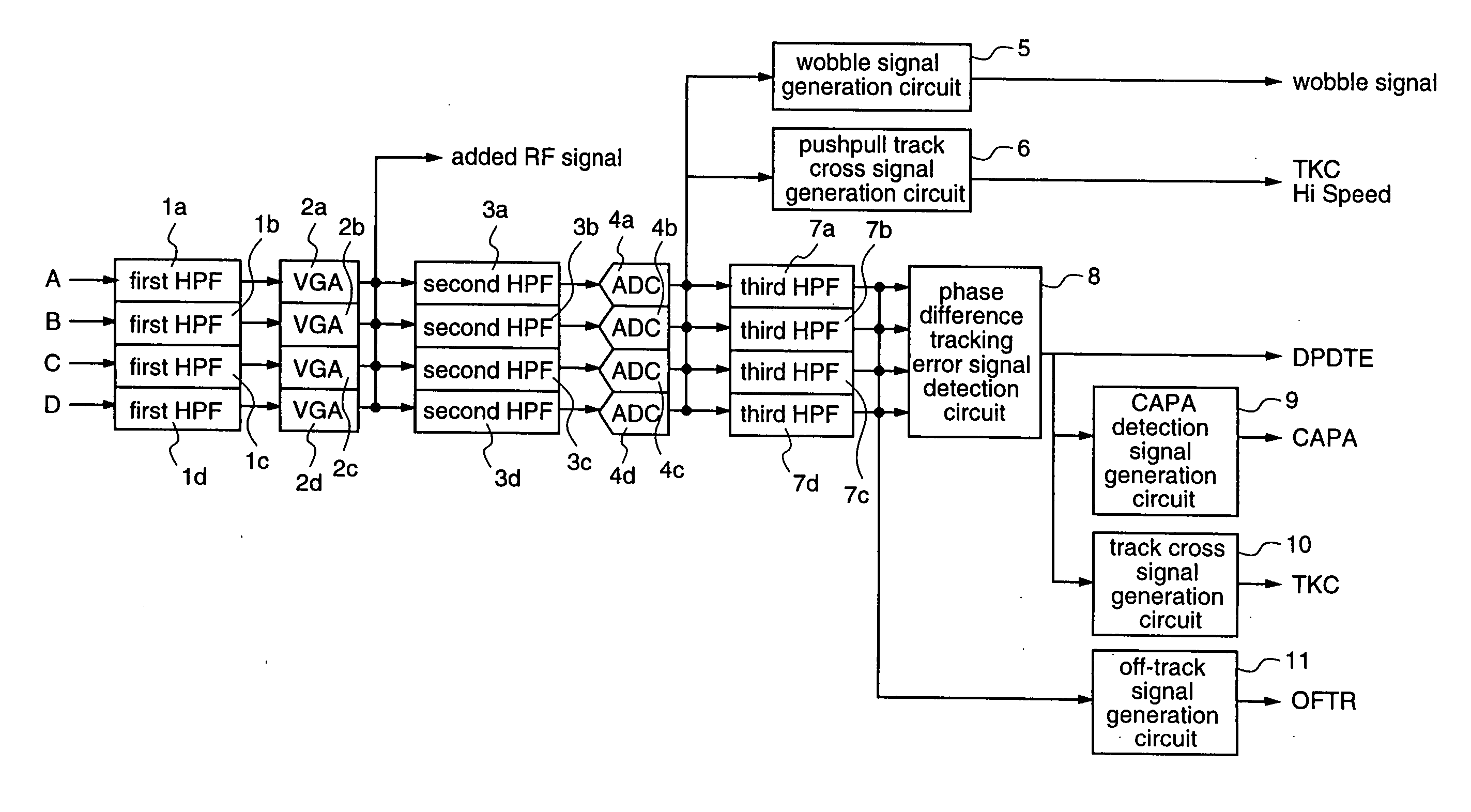
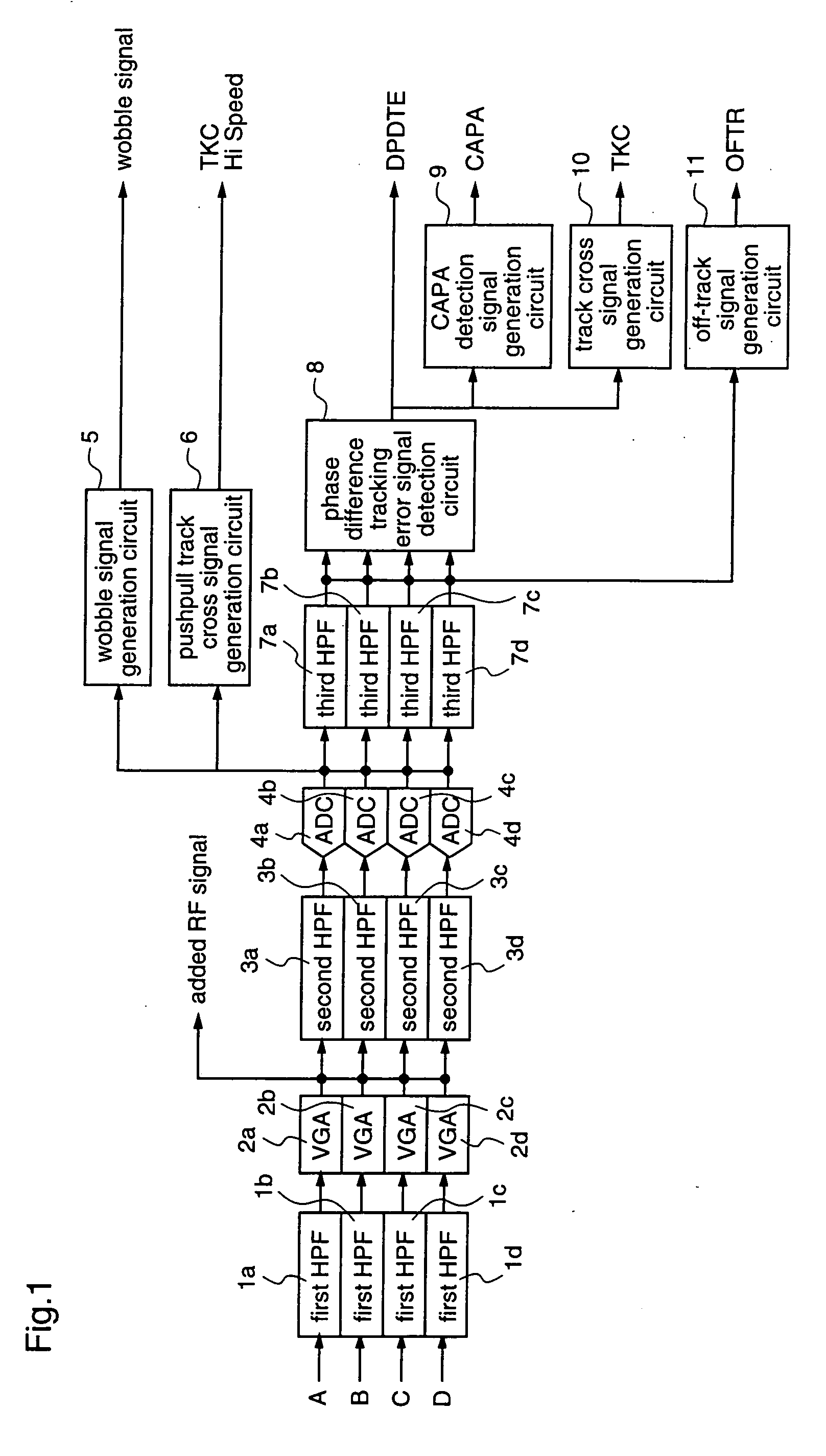
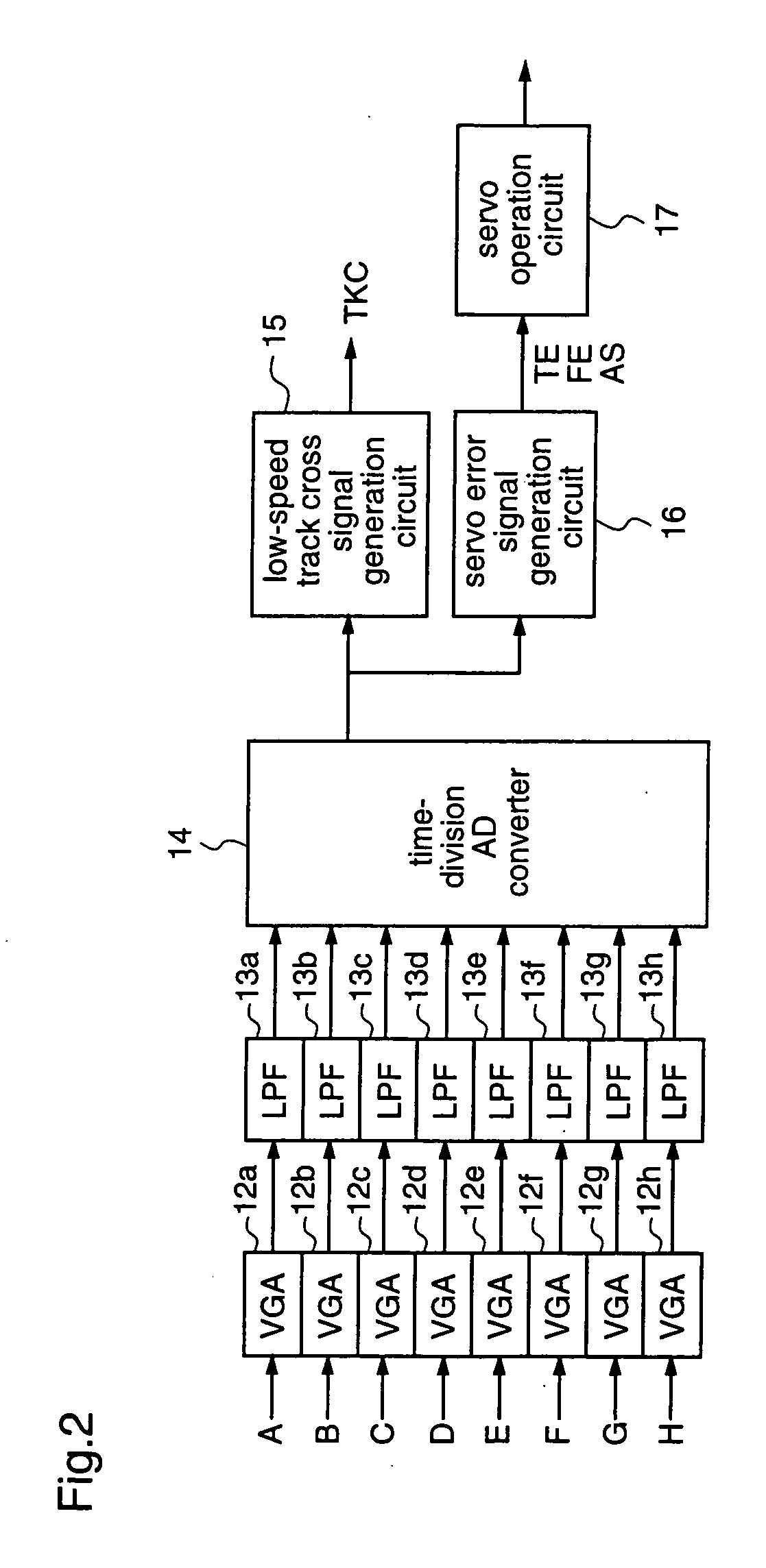
[0128]FIG. 1 is a block diagram illustrating an example of a high frequency band processing circuit of the optical disc device according to the first embodiment of the present invention, and FIG. 2 is a block diagram illustrating an example of a low frequency band processing circuit of the optical disc device according to the first embodiment.

[0129] The high frequency band processing circuit shown in FIG. 1 performs detection of various signals which are required for recording and playback of an optical disc, using high frequency bands of the signals outputted from the pickup, and the low frequency band processing circuit shown in FIG. 2...

embodiment 2

[0181] Next, specific constructions and operations of the servo error signal generation circuit 16 and the servo operation circuit 17 which have been described for the first embodiment using FIG. 2 will be described as a second embodiment of the present invention. In the optical disc device described hereinafter, the servo error signal generation circuit 16 controls the operation timing of arithmetic processing for the signals from the main photodetectors A˜D and the operation timing of arithmetic processing for the signals from the sub photodetectors E˜H separately from each other, and the servo operation circuit 17 performs digital servo operation using the signals generated by the servo error signal generation circuit, thereby generating a drive signal for a driving system.

[0182] FIGS. 4(a) and 4(b) are diagrams for explaining the servo error signal generation circuit and the servo operation circuit of the optical disc device according to the second embodiment of the invention. ...

embodiment 3

[0204] Next, other examples of the servo error signal generation circuit 16 and the servo operation circuit 17, which have been described for the second embodiment, will be described as a third embodiment of the present invention. According to the servo error signal generation circuit 16 and the servo operation circuit 17 of the optical disc device to be described hereinafter, the servo operation circuit 17 is provided with a high-pass phase-lead filter 66 for compensating, by phase compensation, a delay time until the start of the arithmetic processing for the signals from the sub photodetectors E˜H thereby to compensate a phase delay due to the operation delay time for the signals from the sub photodetectors E˜H.

[0205]FIG. 6 is a block diagram illustrating examples of constructions of the servo error signal generation circuit and the servo operation circuit according to the third embodiment.

[0206] In FIG. 6, the servo error signal generation circuit 16 according to the third emb...


PUM


Abstract

An optical disc device according to the present invention is provided with, as shown in FIGS. 1 and 2, a high frequency band processing circuit for removing low frequency components of signals outputted from plural photodetectors of a pickup, and generating various kinds of signals required for recording / playback of an optical disc by digital processing after performing AD conversion by a high-speed low-bit AD converter; and a low frequency band processing circuit for removing high frequency components of the signals outputted from the respective photodetectors of the pickup, and generating various kinds of signals required for recording / playback of an optical disc by digital processing after performing AD conversion by a low-speed high-bit time-division AD converter. Thereby, various kinds of signals required for recording / playback of an optical disc can be generated using a single circuit, whereby the product cost, power consumption, and circuit scale can be reduced.

Description

TECHNICAL FIELD [0001] The present invention relates to an optical disc device for detecting various kinds of signals required for recording and playback of an optical disc, using signals outputted from photodetectors of an optical pickup. BACKGROUND ART [0002]FIG. 20 is a block diagram illustrating the construction of a conventional optical disc device. [0003] With reference to FIG. 20, the conventional optical disc device comprises a pickup 1000, VGA 1001a˜h, HPF 1002a˜d, comparators 1003a˜d, a phase difference tracking error signal detection circuit 1004, an off track signal generation circuit 1005, a differential RF signal generation circuit 1006, a wobble signal generation circuit 1007, a CAPA detection signal generation circuit 1008, a servo error signal generation circuit 1009, a selector 1010, a selector 1011, an LPF 1012, a comparator 1013, an LPF 1014, an LPF 1015, an LPF 1016, a selector 1017, and an ADC 1018. In order to indicate the specific numbers of the VGA 1001, the...

Claims


Application Information

Patent Timeline
IPC IPC(8): G11B7/00G11B7/005G11B7/09
CPCG11B7/005G11B7/09
Inventor KANDA, YOSHIHIROHIRATSUKA, TAKASHIGEOCHIAI, MINORUKIKUCHI, JUN
Owner COLLABO INNOVATIONS INC
Learn More