Class ab CMOS amplifiers

a cmos amplifier and amplifier technology, applied in the field of class ab cmos amplifiers, can solve the problems of large crossover distortion, complex design of ab cmos amplifiers, and difficult to provide a low and controlled quiescent current, and achieve the effect of reducing the variation of quiescent curren

Active Publication Date: 2006-05-25
POWER INTEGRATIONS INC +1
View PDF5 Cites 7 Cited by
  • Summary
  • Abstract
  • Description
  • Claims
  • Application Information

AI Technical Summary

Benefits of technology

[0009] According to one aspect of this invention there is provided a CMOS amplifier having a class AB output stage, the output stage comprising: two complementary transistors having source-drain paths coupled in series between two voltage supply rails and providing an output from a junction therebetween; a level-shifting transistor and a further transistor having source-drain paths coupled in series between the two voltage supply rails for supplying a signal from a junction therebetween to one of said complementary transistors; and a signal input to the other of said complementary transistors and to the level-shifting transistor; the amplifier further comprising a bias circuit for producing a variable bias voltage for said further transistor, the bias circuit comprising: a replica of the level-shifting transistor and a replica of said further transistor coupled in series between the two voltage supply rails in a similar manner to the level-shifting transistor and said further transistor, the replica of said further transistor also being responsive to said variable bias voltage; and a circuit responsive to a voltage at a junction between the replica of the level-shifting transistor and the replica of said further transistor for producing said variable bias voltage in a manner to reduce variations of a quiescent current of the output stage.

Problems solved by technology

An amplifier with a class B output stage can supply a large output current with zero quiescent current, but introduces a large crossover distortion.
Many class AB CMOS amplifiers have the disadvantage of complex design involving relatively large numbers of transistors.
However, especially with typical variations in manufacturing processes, supply voltages, and temperature (referred to as PVT), in such circuits it is difficult to provide a low and controlled quiescent current.

Method used


Image

  • Class ab CMOS amplifiers
  • Class ab CMOS amplifiers
  • Class ab CMOS amplifiers

Examples


Embodiment Construction

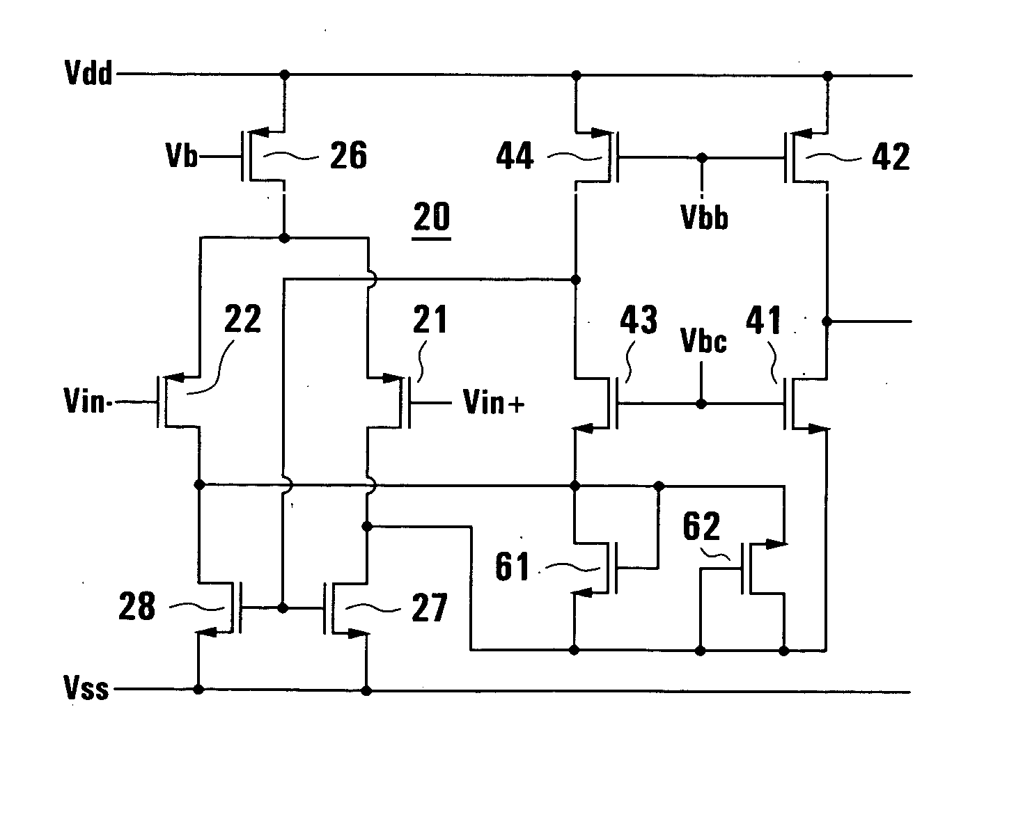
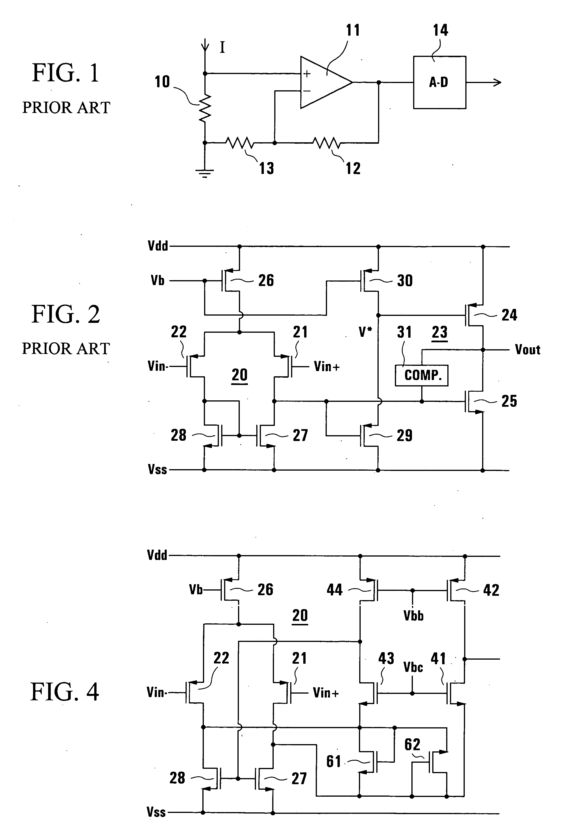
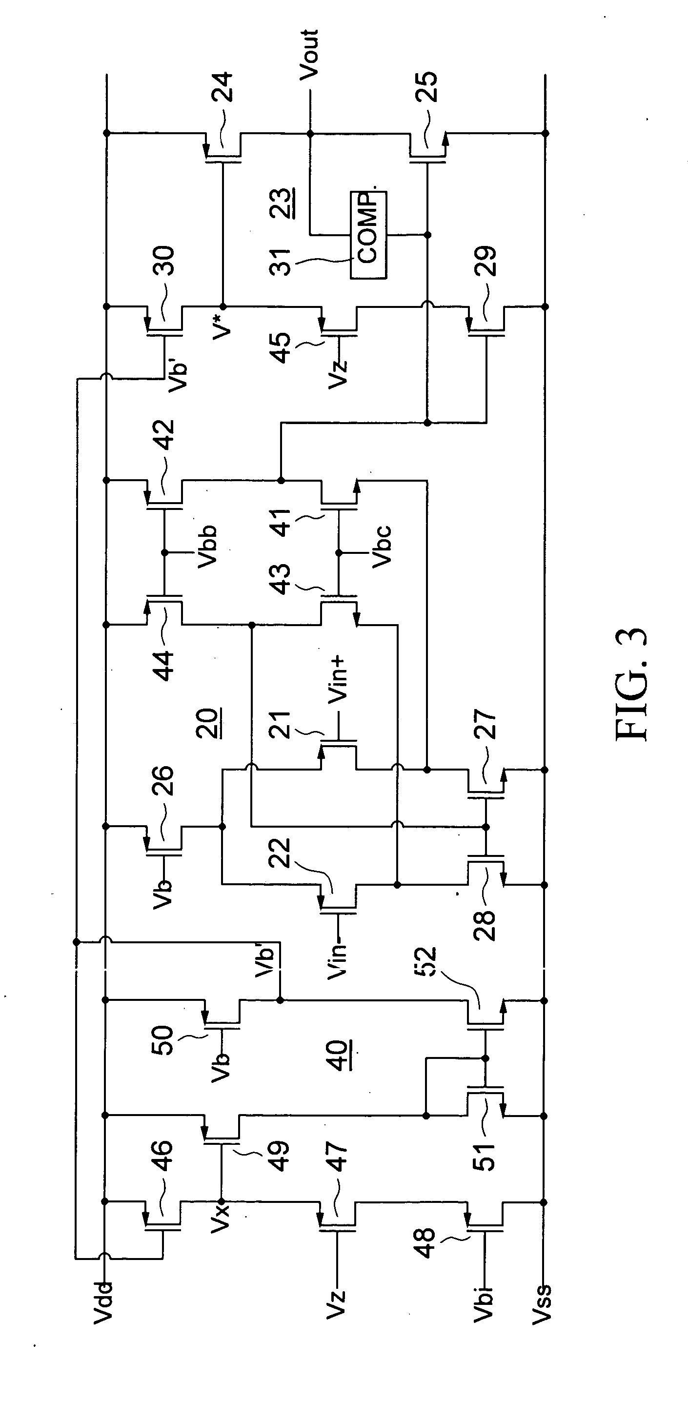
[0028] Referring to the drawings, FIG. 1 illustrates an arrangement in which a resistor 10 of resistance Rs is used for sensing a current I to ground. For example, the current I may be a power supply current which it is desired to monitor, the resistor 10 producing a small voltage Vin+=I.Rs which is supplied to the non-inverting or + input of a differential CMOS amplifier 11. A feedback resistor 12, having a resistance Rf, is connected between an output of the amplifier 11 and its inverting or − input at a voltage Vin−, and a resistor 13 having a resistance Rg is connected between the inverting input and ground, so that an output voltage Vout of the amplifier is ideally equal to (1+Rf / Ri)I.Rs. For example, this output voltage is supplied to an analog-digital (A-D) converter 14 which produces at its output a corresponding digital value.

[0029] It is typically desired for the resistance Rs to be small, e.g. 0.1 Ω or less; consequently the differential input voltage to the amplifier 11...


PUM


Abstract

A class AB output stage of a CMOS amplifier has a level-shifting voltage follower constituted by a level-shifting transistor and a current source. A bias circuit replicates the level-shifting voltage follower in a feedback arrangement to produce a variable bias voltage for the current source of both the main and replica level-shifters. The arrangement serves to control the output voltage of the level-shifter such that it provides the amplifier with a relatively constant quiescent current of the output stage over variations of manufacturing process, supply voltage, and temperature. The level shifting function can be facilitated by a resistive on-state of a power-down transistor between the level-shifting and load transistors.

Description

[0001] This invention relates to CMOS amplifiers, and especially to CMOS amplifiers having a class AB output stage. BACKGROUND [0002] As is well known, an amplifier with a class A output stage can not supply an output current greater than a quiescent current of the output stage. If it is desired to supply an output current greater than the quiescent current, a different class of amplifier is required. An amplifier with a class B output stage can supply a large output current with zero quiescent current, but introduces a large crossover distortion. A class AB output stage provides a compromise, enabling the output current to be greater than the quiescent current without excessive distortion. [0003] It is well known to provide a CMOS amplifier with a class AB output stage. Typically, such an amplifier may be a differential amplifier which has a differential input stage, and may be referred to as an operational amplifier or opamp. [0004] It is desirable for a differential amplifier to ...

Claims


Application Information

Patent Timeline
Patent Type & Authority Applications(United States)
IPC IPC(8): H03F3/45
CPCH03F3/45192H03F3/45659H03F2200/447H03F2203/45668
Inventor COLBECK, ROGER
Owner POWER INTEGRATIONS INC
Why Eureka
Try Eureka