Magnetic random access memory

a random access and memory technology, applied in static storage, digital storage, instruments, etc., can solve the problems of increasing the power consumption of the write operation of the data into the mram, hard to avoid changes of the write current flowing through the selected bit line and the selected word line, and achieve the effect of improving the selectivity of the memory cell and stabilizing the write operation

Inactive Publication Date: 2006-05-11
NEC CORP
View PDF4 Cites 4 Cited by
  • Summary
  • Abstract
  • Description
  • Claims
  • Application Information

AI Technical Summary

Benefits of technology

[0018] An object of the present invention is to provide a magnetic random access memory in which the selectivity of a memory cell can be improved and a write operation can be stabilized.
[0019] Another object of the present invention is to provide a magnetic random access memory in which the selectivity of a memory cell is improved by providing a ferri-magnetic laminate structure for each memory cell.
[0020] Still another object of the present invention is to provide a magnetic random access memory in which the selectivity of a memory cell can be improved by adjusting the film thickness of a non-magnetic layer in a ferri-magnetic laminate structure.

Problems solved by technology

One of the technical problems in the above-mentioned write operation of the data in the MRAM is power consumption.
The large currents increase the power consumption in the write operation of the data into the MRAM.
Another technical problem in the write operation of the data in the MRAM is selectivity of the selected memory cell.
However, it is hard to avoid changes of the write currents flowing through the selected bit line and the selected word line and the asteroid curve because of a variation in a manufacturing process and a variation in use environment of the MRAM.
The changes degrade the selectivity of the selected memory cell, and a malfunction may be caused in which an undesired data is written in the non-selected memory cell in the write operation of data.

Method used


Image

  • Magnetic random access memory
  • Magnetic random access memory
  • Magnetic random access memory

Examples


first embodiment

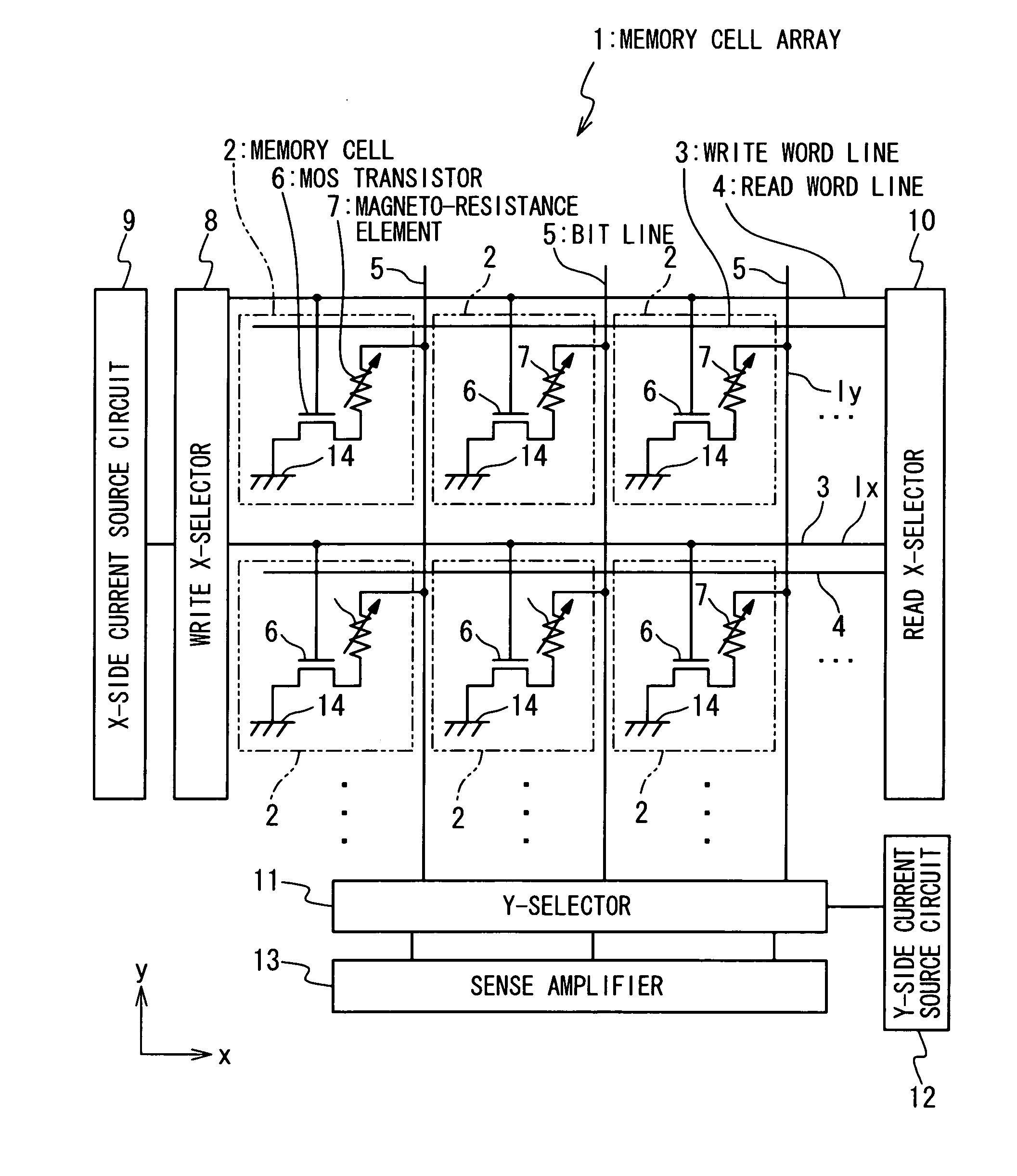
[0081] As shown in FIG. 4, the MRAM according to the first embodiment of the present invention is provided with a memory cell array 1 in which memory cells 2 are arranged in a matrix. Write word lines 3 extending in the X-axis direction, read word lines 4 provided in parallel with the write word line 3 and bit lines 5 extending in the Y-axis direction are arranged in the memory cell array 1. The X-axis direction is substantially perpendicular to the Y-axis direction. Herein, it should be noted that the term “X axis direction” contains both a positive direction of the X-axis (+X direction) and a negative direction of X-axis (−X direction), and the term “Y axis direction” contains both a positive direction of the Y-axis (+Y direction) and a negative direction of the Y-axis (−Y direction). The memory cells 2 are respectively provided at the intersections of the write word lines 3 and the bit lines 5.

[0082] The memory cell 2 contains a MOS transistor 6 and a magneto-resistance element ...

second embodiment

[0116]FIG. 14 shows the MRAM according to the second embodiment of the present invention. The MRAM according to the second embodiment has a circuit configuration in which the transistor is not contained in the memory cell, and which contains so called a cross point cell array.

[0117] The MRAM according to the second embodiment is provided with the cross point cell array 41 in which the memory cells 42 are arranged in a matrix. Word lines 43 extending in the X axis direction and bit lines 44 extending in the Y axis direction are arranged on the cross point cell array 41. The memory cells 2 are respectively formed at the intersections of the word lines 43 and the bit lines 44. The memory cell 42 contains a magneto-resistance element 45. The magneto-resistance element 45 has reversible spontaneous magnetization and holds data according to the direction of the spontaneous magnetization. Each of the magneto-resistance elements 45 is interposed between the word line 43 and the bit line 44...

third embodiment

[0142] Next, with reference to FIGS. 21 and 22, the MRAM due to the third embodiment of the present invention will be described. As shown in FIGS. 21 and 22, in the MRAM due to the third embodiment, the arrangement of the magneto-resistance element 45 and the ferri-magnetic laminate structure 55 are changed. As shown in FIG. 21, in the sectional structure of the memory cell 42, the positions of the magneto-resistance element 45 and the ferri-magnetic laminate structure 55 are exchanged. As shown in FIG. 22, the ferri-magnetic laminate structure 55 has a substantial elliptical plane shape. The long axis of the ferri-magnetic laminate structure 55 is inclined by an angle θ from the X-axis. Typically, the angle θ is 45 degrees. The structure of other portion of the MRAM according to the third embodiment is the same as the second embodiment. The circuit of the MRAM according to the third embodiment is the same as the circuit of the MRAM according to the second embodiment shown in FIG. 1...


PUM


Abstract

A magnetic random access memory is composed of a plurality of first signal lines provided to extend in a first direction, a plurality of second signal lines provided to extend in a second direction substantially perpendicular to the first direction, a plurality of memory cells respectively provided at the intersections of the plurality of first signal lines and the plurality of second signal lines, and a plurality of magnetic structures respectively provided to the plurality of memory cells. Each of the plurality of memory cells has a magneto-resistance element containing a spontaneous magnetization layer which has a first threshold function, and the direction of the spontaneous magnetization of the spontaneous magnetization layer is reversed when an element applied magnetic field having the intensity equal to or larger than a first threshold function value is applied. Each of the plurality of magnetic structures has a second threshold function, and generates a magnetic structure magnetic field in response to a structure-applied magnetic field. When the structure-applied magnetic field has the intensity equal to or larger than the second threshold function value, a third magnetic field is generated as the magnetic structure magnetic field. When the structure applied magnetic field has the intensity less than the second threshold function value, a fourth magnetic field is generated which is weaker than the third magnetic field as the magnetic structure magnetic field. A first write current supplied to one of the plurality of first signal lines as a first selected signal line, and a first magnetic field is generated. A second write current is supplied to one of the plurality of second signal lines as a second selected signal line, and a second magnetic field is generated. A first synthetic magnetic field of the first magnetic field and the second magnetic field is applied to the magnetic structure as the structure applied magnetic field. The element applied magnetic field having the intensity equal to or larger than the first threshold function value is applied to the selected memory cell provided at the intersection of the first selected signal line and the second selected signal line. A second synthetic magnetic field of the first synthetic magnetic field and the magnetic structure magnetic field is generated as the element applied magnetic field such that the element applied magnetic field having the intensity less than the first threshold function value is applied to each of non-selected memory cells other than the selected memory cell.

Description

FIELD OF INVENTION [0001] The present invention relates to a magnetic random access memory. BACKGROUND ART [0002] A magnetic random access memory (MRAM) collects attention as a nonvolatile memory in which a high-speed write operation can be carried out and the number of times of rewrite is large. [0003]FIG. 1 shows a typical MRAM disclosed in U.S. Pat. No. 5,640,343. The MRAM contains a memory cell array in which memory cells 101 are arranged in a matrix. The memory cell 101 is interposed between a word line 102 extending in an X axis direction (word line direction), and a bit line 103 extending in a Y axis direction (bit line direction). [0004] As shown in FIGS. 2A and 2B, each memory cell 101 contains a magneto-resistance element (spin valve). The magneto-resistance element has a pinned layer 104 and a free layer 105 which are made of ferromagnetic material, and a non-magnetic spacers layer 106 interposed between the pinned layer 104 and the free layer 105. The pinned layer 104 ma...

Claims


Application Information

Patent Timeline
Patent Type & Authority Applications(United States)
IPC IPC(8): G11C11/00G11C11/16
CPCG11C11/16
Inventor SUGIBAYASHI, TADAHIKOHONDA, TAKESHISAKIMURA, NOBORUMATSUTERA, HISAOKAMIJO, ATSUSHISHIMURA, KENICHI
Owner NEC CORP
Why Eureka
Try Eureka