White OLEDs with a color-compensated electroluminescent unit
a color-compensated, electroluminescent unit technology, applied in the direction of discharge tube/lamp details, discharge tube luminescnet screens, other domestic articles, etc., can solve the problems of difficult to achieve a wide emission with a balanced intensity from red, green, and only one lel, so as to achieve a wide range of emission and reduce the drive voltage , the effect of fewer fabrication steps
- Summary
- Abstract
- Description
- Claims
- Application Information
AI Technical Summary
Benefits of technology
Problems solved by technology
Method used
Image
Examples
example 1
Comparative
[0082] The preparation of a comparative white OLED is as follows: A˜1.1 mm thick glass substrate coated with a transparent indium-tin-oxide (ITO) conductive layer was cleaned and dried using a commercial glass scrubber tool. The thickness of ITO is about 42 nm and the sheet resistance of the ITO is about 68 Ω / square. The ITO surface was subsequently treated with oxidative plasma to condition the surface as an anode. A layer of CFx, 1 nm thick, was deposited on the clean ITO surface as the hole-injecting layer by decomposing CHF3 gas in an RF plasma treatment chamber. The substrate was then transferred into a vacuum deposition chamber for deposition of all other layers on top of the substrate. The following layers were deposited in the following sequence by evaporation from a heated boat under a vacuum of approximately 10−6 Torr:
[0083] 1. EL Unit:
[0084] a) an HTL, about 90 nm thick, including “4,4′-bis[N-(1-naphthyl)-N-phenylamino]biphenyl” (NPB);
[0085] b) a first LEL,...
example 2
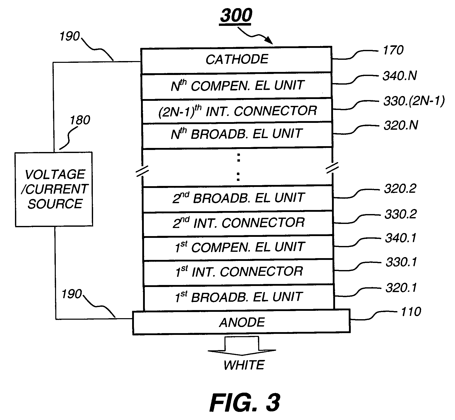
[0091] A tandem white OLED was constructed in accordance with the present invention as described in FIG. 4. The fabrication methods used in Example 2 are similar to those used in Example 1, and the deposited layer structure is:
[0092] 1. 1st EL Unit (1st Broadband EL Unit):
[0093] a) an HTL, about 30 nm thick, including NPB;
[0094] b) a first LEL, 30 nm thick, including 70 vol. % NPB, 29.5 vol. % rubrene, and 0.5 vol. % “5,10,15,20-tetraphenyl-bisbenz[5,6]indeno[1,2,3-cd: 1′,2′,3′-1 m]perylene” (red emitting layer);
[0095] c) a second LEL, 40 nm thick, including 85 vol. % “2-(1,1-dimethyethyl)-9,10-di-2-naphthalenyl anthracene” (TBADN), about 13.5 vol. % NPB, and 1.5 vol. % “2,5,8,11-tetra-t-butylperylene (TBP)” (blue emitting layer); and
[0096] d) an ETL, 10 nm thick, including Alq.
[0097] 2. 1st Intermediate Connector:
[0098] a) an n-type doped organic layer, 10 nm thick, including Alq doped with about 1.2 vol. % lithium; and
[0099] b) a metal compound layer, 2 nm thick, including...
PUM
| Property | Measurement | Unit |
|---|---|---|
| Sheet resistance | aaaaa | aaaaa |
| Color | aaaaa | aaaaa |
| Structure | aaaaa | aaaaa |
Abstract
Description
Claims
Application Information
 - R&D
- Intellectual Property
- Life Sciences
- Materials
- Tech Scout
- Unparalleled Data Quality
- Higher Quality Content
- 60% Fewer Hallucinations
Browse by: Latest US Patents, China's latest patents, Technical Efficacy Thesaurus, Application Domain, Technology Topic, Popular Technical Reports.
© 2025 PatSnap. All rights reserved.Legal|Privacy policy|Modern Slavery Act Transparency Statement|Sitemap|About US| Contact US: help@patsnap.com


