Liquid crystal display device and method of manufacturing the same

Inactive Publication Date: 2006-04-13
SAMSUNG DISPLAY CO LTD
View PDF12 Cites 5 Cited by
  • Summary
  • Abstract
  • Description
  • Claims
  • Application Information

AI Technical Summary

Benefits of technology

[0011] In exemplary embodiments of the present invention. the above problems are solved by reducing a transition time and decreasing a transition voltage by facilitating transition from splay alignment to band alignment without deteriorating optical characteristics of liquid crystal in an OCB mode liquid crystal display device.

Problems solved by technology

In the OCB mode liquid crystal display device, a very high voltage and a long time are typically required for changing the initially splay-aligned liquid crystal molecules to have the band alignment.
Accordingly, an optical overshoot phenomenon occurs, thereby causing a deterioration of image quality.
However, in such a liquid crystal display device, there is a problem that much labor is required for arrangement of the upper and lower substrates in order to accurately position the transition seed areas, and there is also a problem that electro-optical characteristics become uneven inside a pixel since areas having different alignment exist in the pixel.

Method used


Image

  • Liquid crystal display device and method of manufacturing the same
  • Liquid crystal display device and method of manufacturing the same
  • Liquid crystal display device and method of manufacturing the same

Examples


Embodiment Construction

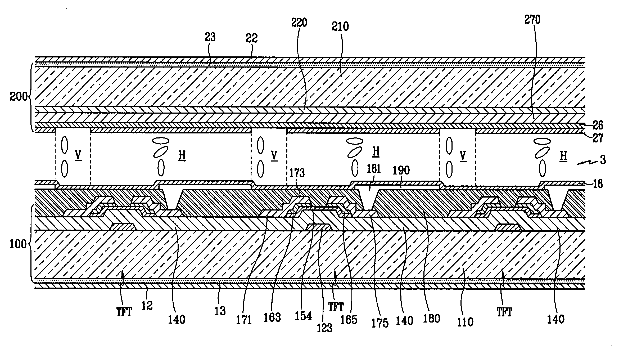
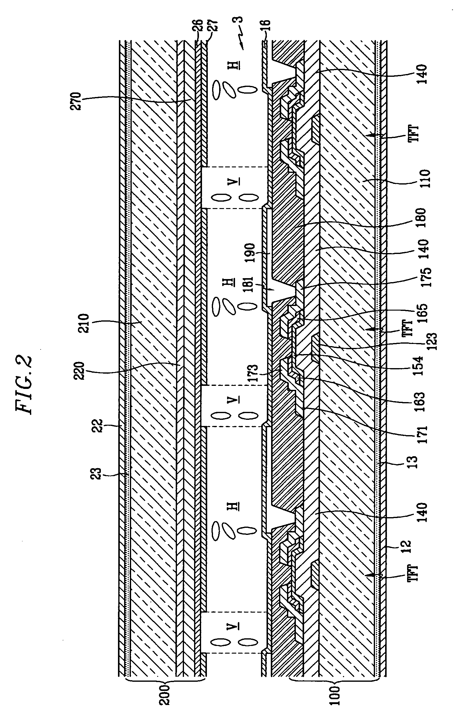
[0038] In the following detailed description, only certain exemplary embodiments of the present invention are shown and described, simply by way of illustration. As those skilled in the art would realize, the described embodiments may be modified in various different ways, all without departing from the spirit or scope of the present invention. Accordingly, the drawings and description are to be regarded as illustrative in nature, and not restrictive. There may be parts shown in the drawings, or parts not shown in the drawings, that are not discussed in the specification as they are not essential to a complete understanding of the invention. Like reference numerals designate like elements.

[0039] In the drawings, thicknesses are enlarged to clearly express various layers and areas. When it is described that one element such as a layer, a film, an area, a plate, etc. is formed on another element, it means that one element exists right on another element or that one element exists on ...


PUM


Abstract

A liquid crystal display device having vertical alignment films formed on pixel electrodes of a thin film transistor substrate and a common electrode of a common electrode substrate, and horizontal alignment films formed in a shape of plural belts on the vertical alignment films. The horizontal alignment film of the thin film transistor substrate and the horizontal alignment film of the common electrode substrate are substantially perpendicular to each other. Accordingly, a liquid crystal layer interposed between the two substrates includes a splay area, a homeotropic area, and hybrid area, wherein the hybrid area is disposed around the splay area and the homeotropic area. Since the hybrid area serves as an alignment transition seed, the liquid crystal molecules of the splay area can be easily changed to have a band alignment. Therefore, it is possible to decrease an alignment transition voltage and to enhance an alignment transition speed.

Description

CROSS-REFERENCE TO RELATED APPLICATIONS [0001] This application claims priority to and the benefit of Korean Patent Application No. 10-2004-0081628 filed on Oct. 13, 2004 in the Korean Intellectual Property Office, the entire content of which is incorporated herein by reference. BACKGROUND OF THE INVENTION [0002] (a) Field of the Invention [0003] The present invention relates to a liquid crystal display device, and more particularly, to an optically compensated bend (hereinafter, referred to as OCB) mode liquid crystal display device. [0004] (b) Description of Related Art [0005] In liquid crystal display devices, a liquid crystal material is interposed between an upper substrate on which a common electrode, etc. are formed and a lower substrate on which thin film transistors, pixel electrodes, etc. are formed. In a liquid crystal display device, an electric field is formed by applying different potentials to the pixel electrodes and the common electrode, thereby varying alignment of...

Claims


Application Information

Patent Timeline
IPC IPC(8): G02F1/1337
CPCG02F1/133753G02F1/133784G02F1/1395G02F2001/133738G02F2001/133742G02F2001/133761G02F1/133738G02F1/133742G02F1/133761G02F1/1337
Inventor JUNG, TAE-HYEOGKIM, KEE-DOOHEO, HAE-JIN
Owner SAMSUNG DISPLAY CO LTD
Why Eureka
Try Eureka