
Method and apparatus for mounting and removing an electronic component

a technology for electronic components and mounting methods, applied in sustainable manufacturing/processing, program control, instruments, etc., can solve problems such as short circuit of solders, reduced reliability of connection, and accumulation of thermal stresses in substrates, so as to simplify preprocessing and reduce stress and costs , the effect of enhancing reliability

Inactive Publication Date: 2006-04-13
FUJITSU LTD
View PDF4 Cites 42 Cited by
  • Summary
  • Abstract
  • Description
  • Claims
  • Application Information

AI Technical Summary

Benefits of technology

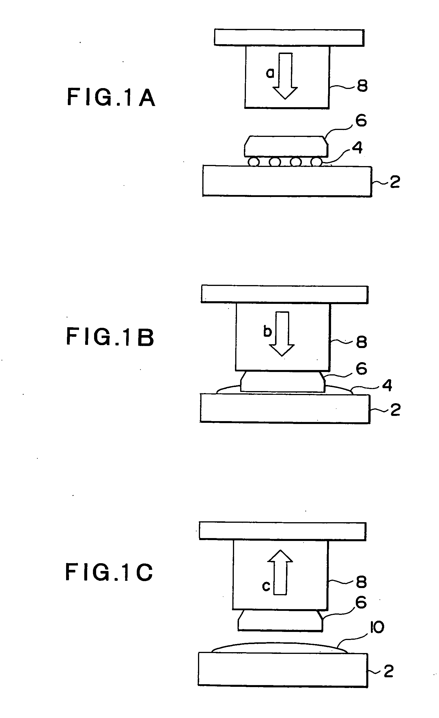
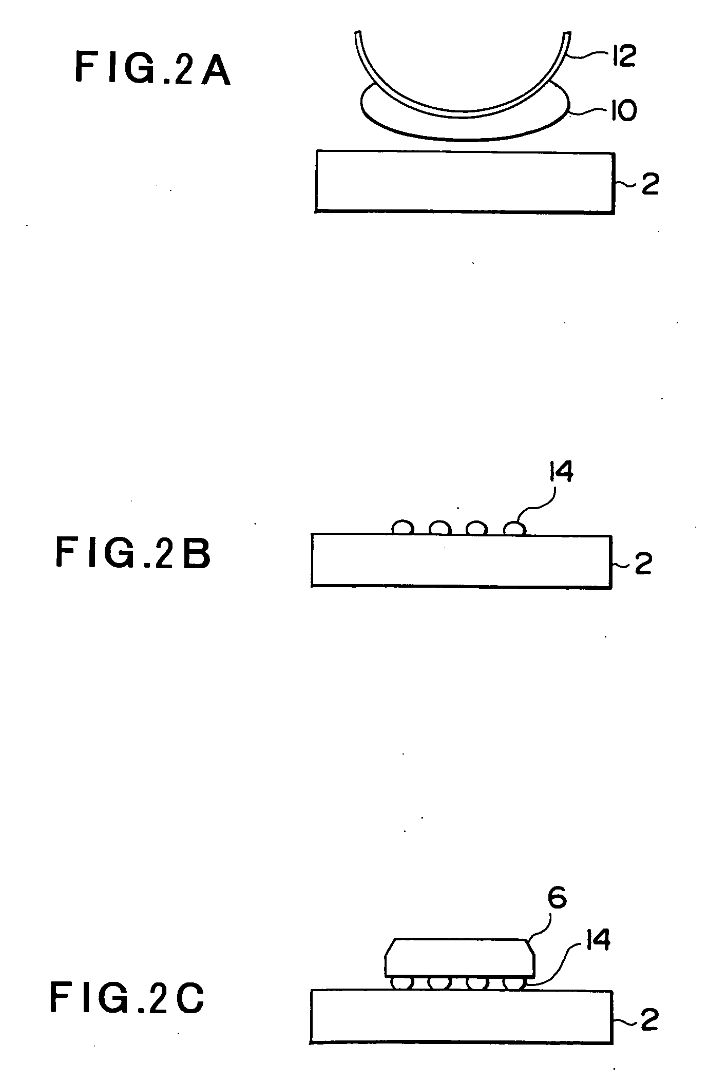
[0015] More particularly, an object of the present invention is to provide a method and an apparatus for mounting and removing electronic components, which can constrain thermal stresses generated on a substrate. Another object of the present invention is to provide a method and an apparatus for removing electronic components, which enable reuse of residual solder.
[0032] Also, according to the apparatus for removing the electronic component of the present invention, the electronic component can be removed with one-time heating without generating stresses to the substrate, and the residual solder in the reusable state can be formed, which contributes to simplification of preprocessing and the like to enable fast and easy remounting.

Problems solved by technology

If a bonding portion of a bear chip has narrow gaps, when an error occurs in the position control of the tool, solder may be short-circuited and the residual solder in the short-circuit state must be removed by sufficient cleaning processing before replacing the bear chip.
Although the preliminary-solder processing is used for ensuring connectivity between the substrate and bear chip, thermal stresses are accumulated in the substrate due to the preliminary-solder processing and the reliability of the connection may be reduced.
Also, since the reflow processing of the entire package gives great thermal stresses to the substrate, if a member with limited heat resistance is mounted on the package, reprocessing is difficult and inspection costs are increased for such as the failure analysis of the bear chips at the time of mounting.
These problems cannot be solved by technologies disclosed in the prior patent documents described above.

Method used


Image

  • Method and apparatus for mounting and removing an electronic component
  • Method and apparatus for mounting and removing an electronic component
  • Method and apparatus for mounting and removing an electronic component

Examples


first embodiment

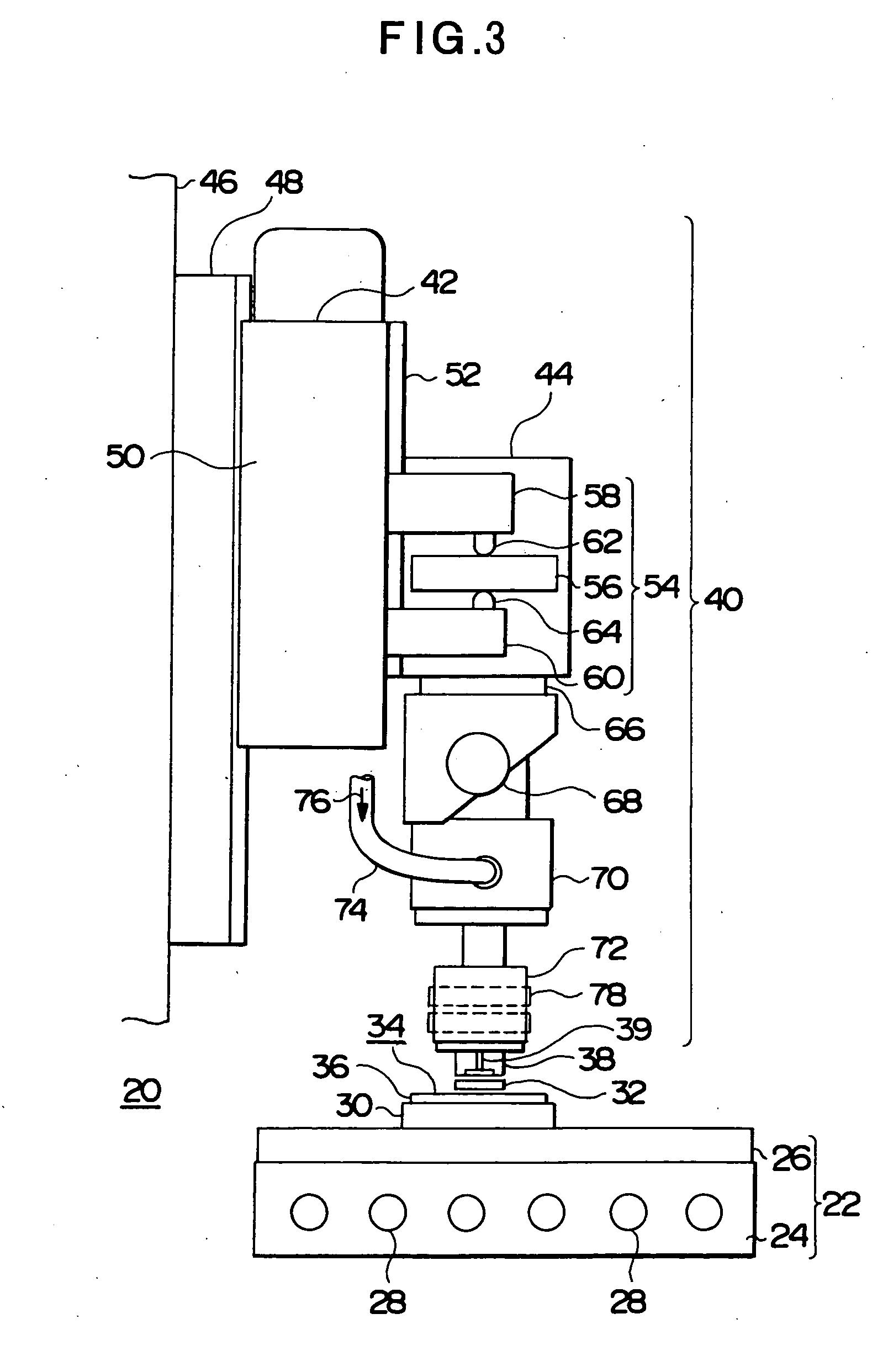
[0053] A first embodiment of the present invention is described with reference to FIG. 3 to FIG. 5. FIG. 3 to FIG. 5 shows a bonding apparatus as an embodiment of a method and an apparatus for mounting and removing electronic components of the present invention; FIG. 3 is a side view showing a head unit and a control table; FIG. 4 is a front view of the head unit; and FIG. 5 is a block diagram showing a configuration of a control unit.

[0054] A bonding apparatus 20 is comprised of a control table 22 movable in the X and Y directions (e.g., horizontal direction); the control table 22 is comprised of, for example, a heating platform portion 24 and a package loading platform 26; and the heating platform portion 24 is comprised of a heater 28 as a first heating unit with in a chassis made up of corrosion resistant metal such as stainless steel. The package loading platform 26 is comprised of a flat loading surface made up of quartz glass. The package loading platform 26 is equipped with...

second embodiment

[0065] Then, as a method for mounting electronic components which is a second embodiment of the present invention, the reflow processing is described with reference to FIG. 6 to FIGS. 9A and 9B. FIG. 6 is a process chart showing an operation sequence of the reflow processing, and FIGS. 7A and 7B to FIGS. 9A and 9B are diagrams showing an operation sequence.

[0066] The reflow processing is constituted by preprocessing, a preparation operation, a height control / reference position detection operation, a bonding-portion heating and height-control operation, and a termination operation. In preprocessing, flux is applied to the bear chip 32 (process P1) and the entire package 34 is preheated (process P2). In this case, the flux is applied to the entire area of the solder bump connection portion of the bear chip 32 and the package 34 is preheated by heating the control table 22. In this preheating, in order to reduce thermal distortion due to difference in temperature, the preheating tempe...

third embodiment

[0082] Then, a third embodiment of the present invention, i.e., a method for removing electronic components is described with reference to FIG. 13 to FIGS. 16A and 16B. FIG. 13 is a process chart showing an operation sequence of remove processing and FIGS. 14A and 14B to FIGS. 16A and 16B are diagrams showing an operation of the head unit 40.

[0083] The remove processing is constituted by preprocessing, a preparation operation, a height control / reference position detection operation, a bear-chip remove operation, and a termination operation. In preprocessing, filling with flux (process P21) and preheating of the entire package 34 (process P22) are performed. The entire connection portion of the solder bumps 114 of the bear chip 32 is filled with the flux utilizing a capillary phenomenon (process P21) and, at this point, preheating the package 34 facilitates the filling with the flux. The package is preheated by heating the control table 22 and, in this preheating, in order to reduce...


PUM

PropertyMeasurementUnit
temperatureaaaaaaaaaa
diameteraaaaaaaaaa
diameteraaaaaaaaaa

Abstract

A method and an apparatus are provided for mounting and removing electronic components using solder bumps while constraining thermal stresses to a substrate. The method and apparatus for mounting and removing an electronic component (bear chip 32) to be soldered onto the substrate with solder bumps 114 is configured to move the electronic component to detect contact of the solder bumps with the substrate or contact of a tool (chuck unit 38) with the electronic component, to define the contact as an original point for raising a heating temperature of the electronic component and the substrate from the heating temperature to a maximum heating temperature HTm as well as move the electronic component in conformity with the temperature rising, and to move the electronic component from a position where the maximum heating temperature is achieved to a mounting height of the substrate.

Description

CROSS-REFERENCE TO RELATED APPLICATIONS [0001] This application is a continuation of International Application No. PCT / JP03 / 06748, filed on May 29, 2003, now pending, herein incorporated by reference.BACKGROUND OF THE INVENTION [0002] 1. Field of the Invention [0003] The present invention relates generally to a method and an apparatus for mounting and removing semiconductor devices such as bear chips, flip chip components and other various electronic components connected to a substrate with solder bumps and, more particularly, to a method and an apparatus for mounting and removing electronic components suitable for various processing such as reworking, replacing and repairing bear chips mounted on a resin substrate with the use of solder bumps. [0004] As a mounting technology for bear chips, the C4 (Controlled Collapse Chip Connection) flip chip wiring technology is used and, in this C4 flip chip wiring technology, connecting protruding terminals (micro bumps) are formed with narrow...

Claims


Application Information

Patent Timeline
Patent Type & Authority Applications(United States)
IPC IPC(8): B23K20/00B23K1/018B23K3/06H05K3/34
CPCB23K1/018B23K3/0623B23K2201/40B23Q15/22G05B2219/37407G05B2219/45235H01L21/67144H01L24/75H01L24/81H01L2224/16H01L2224/75H01L2224/75251H01L2224/75252H01L2224/75743H01L2224/8121H01L2224/81815H01L2924/3025H01L2924/3511H05K3/3436H05K3/3494H05K2203/163H01L2924/01005H01L2924/01006H01L2924/01033H01L2924/01067H01L2924/01075H01L2224/16225B23K2101/40H01L24/799H01L24/98H01L2224/05001H01L2224/05026H01L2224/05568H01L2224/75502H01L2224/81048H01L2924/00014Y02P70/50H01L2224/05005H01L2224/05541H01L2224/05599H01L2224/05099
Inventor SATO, TOSHIHISA
Owner FUJITSU LTD
Learn More