Printed circuit board and method of fabricating same

Inactive Publication Date: 2006-04-06
SAMSUNG ELECTRO MECHANICS CO LTD
View PDF9 Cites 14 Cited by
  • Summary
  • Abstract
  • Description
  • Claims
  • Application Information

AI Technical Summary

Benefits of technology

[0028] Therefore, the present invention has been made keeping in mind the above disadvantages occurring in the prior arts, and an object of the present invention is to provide a PCB, in which an internal circuit of a via hole is not interrupted, and a method of fabricating the same.

Problems solved by technology

However, since the thick electroless copper plating layer 20 (growing for 30 min at a growth speed of about 10 μm / h) must be etched, undesirably, the circuit pattern is over-etched.

Method used


Image

  • Printed circuit board and method of fabricating same
  • Printed circuit board and method of fabricating same
  • Printed circuit board and method of fabricating same

Examples


Embodiment Construction

[0048] Hereinafter, a detailed description will be given of a PCB and a method of fabricating the same according to the present invention with reference to the drawings.

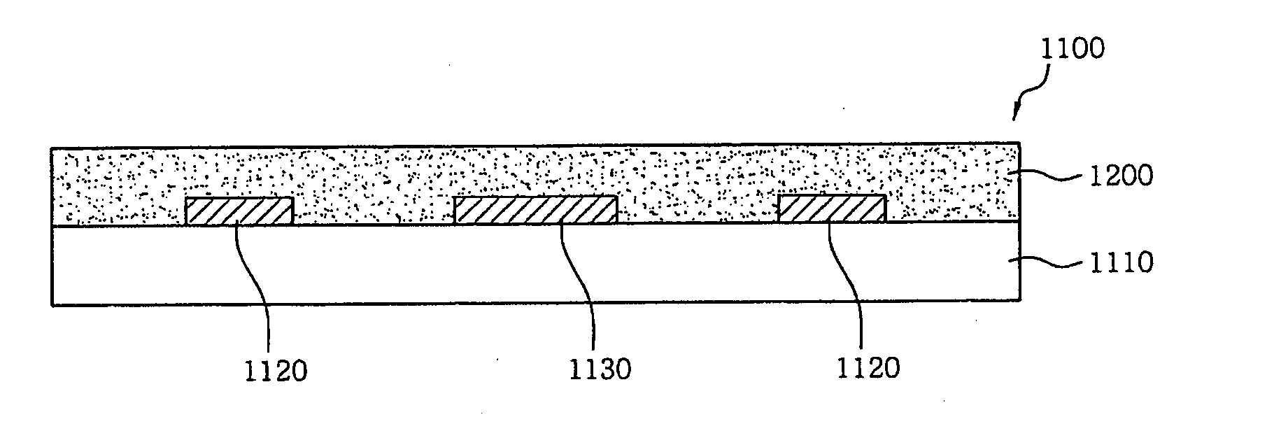
[0049]FIGS. 4a and 4j are sectional views illustrating the fabrication of a PCB according to the present invention, and FIG. 5 is a partially enlarged view of a portion B which is marked by a dotted circle of FIG. 4j. In the drawings, only one side of the PCB is illustrated, but in practice, both sides of the PCB are processed.

[0050] As shown in FIG. 4a, a substrate, that is, a copper clad laminate 1100, is provided, in which a first circuit pattern 1120 and a lower land 1130 are formed on an insulating resin layer 1110. Subsequently, an insulating layer 1200 (for example, prepreg) is laminated on the substrate 1100.

[0051] In this respect, the copper clad laminate used as the substrate 1100 may be classified into a glass / epoxy copper clad laminate, a heat-resistant resin copper clad laminate, a paper / phenol copper...


PUM


Abstract

Disclosed is a PCB which includes an insulating layer. At least one via hole is formed through the insulating layer. A first electroless plating layer is formed on a wall of the via hole and on at least one side of the insulating layer so as to have a predetermined pattern, and is etched at its edge portion corresponding to an edge portion of the pattern in a dimension that is in proportion to a thickness thereof. A second electroless plating layer is formed on the first electroless plating layer. An electrolytic plating layer is formed on the second electroless plating layer, and is etched at its edge portion in a dimension that is in proportion to the thickness of the first electroless plating layer.

Description

INCORPORATION BY REFERENCE [0001] The present application claims priority under 35 U.S.C. §119 to Korean Patent Application No. 2004-79132 filed on Oct. 5, 2004. The content of the application is incorporated herein by reference in its entirety. BACKGROUND OF THE INVENTION [0002] 1. Field of the Invention [0003] The present invention relates, in general, to a printed circuit board (PCB) and a method of fabricating the same and, more particularly, to a PCB and a method of fabricating the same, in which an electroless copper plating process is repeated twice to prevent interruption of an internal circuit of a via hole and to form a fine circuit pattern. [0004] 2. Description of the Prior Art [0005] As a technology for coping with a highly dense semiconductor chip and a high signal transmission speed of the semiconductor chip, demand for direct mounting of a semiconductor chip on a PCB is lately growing instead of CSP (chip-sized package) or wire bonding mounting technologies. To direc...

Claims


Application Information

Patent Timeline
IPC IPC(8): H05K1/11H01R12/04
CPCH05K3/108H05K3/388H05K3/421H05K3/4644H05K3/4661H05K2201/09563H05K2203/072H05K2203/0723H05K2203/1476H05K1/11H05K3/18
Inventor KIM, SEUNG CHUL
Owner SAMSUNG ELECTRO MECHANICS CO LTD
Why Eureka
Try Eureka