Wiring pattern formation method, wiring pattern, and electronic device
- Summary
- Abstract
- Description
- Claims
- Application Information
AI Technical Summary
Benefits of technology
Problems solved by technology
Method used
Image

Examples
first embodiment
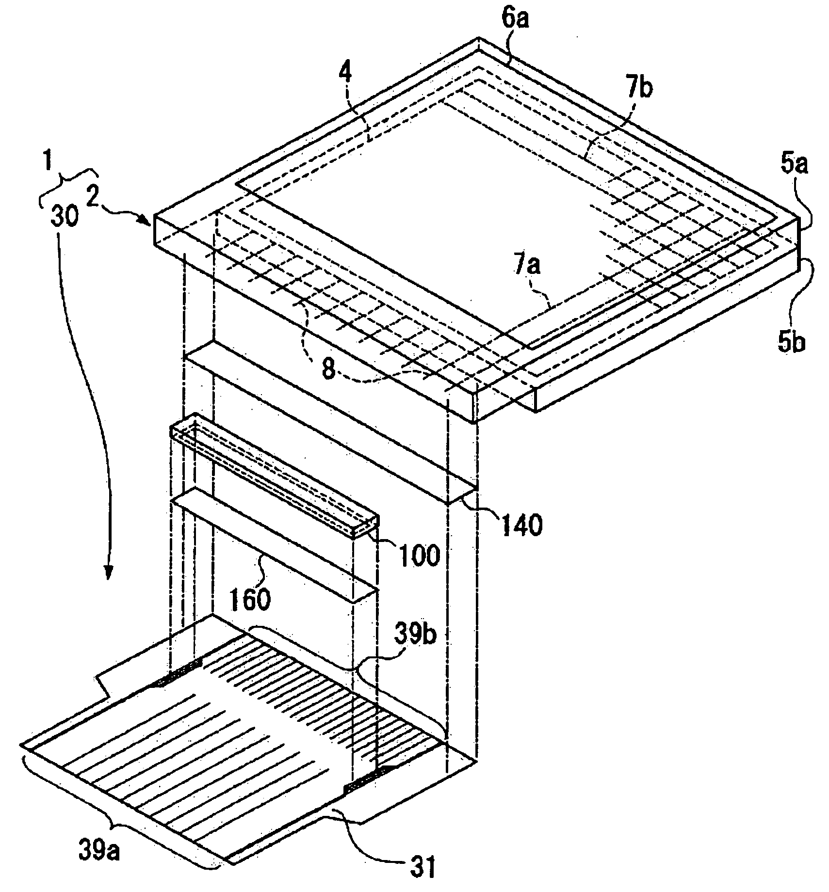
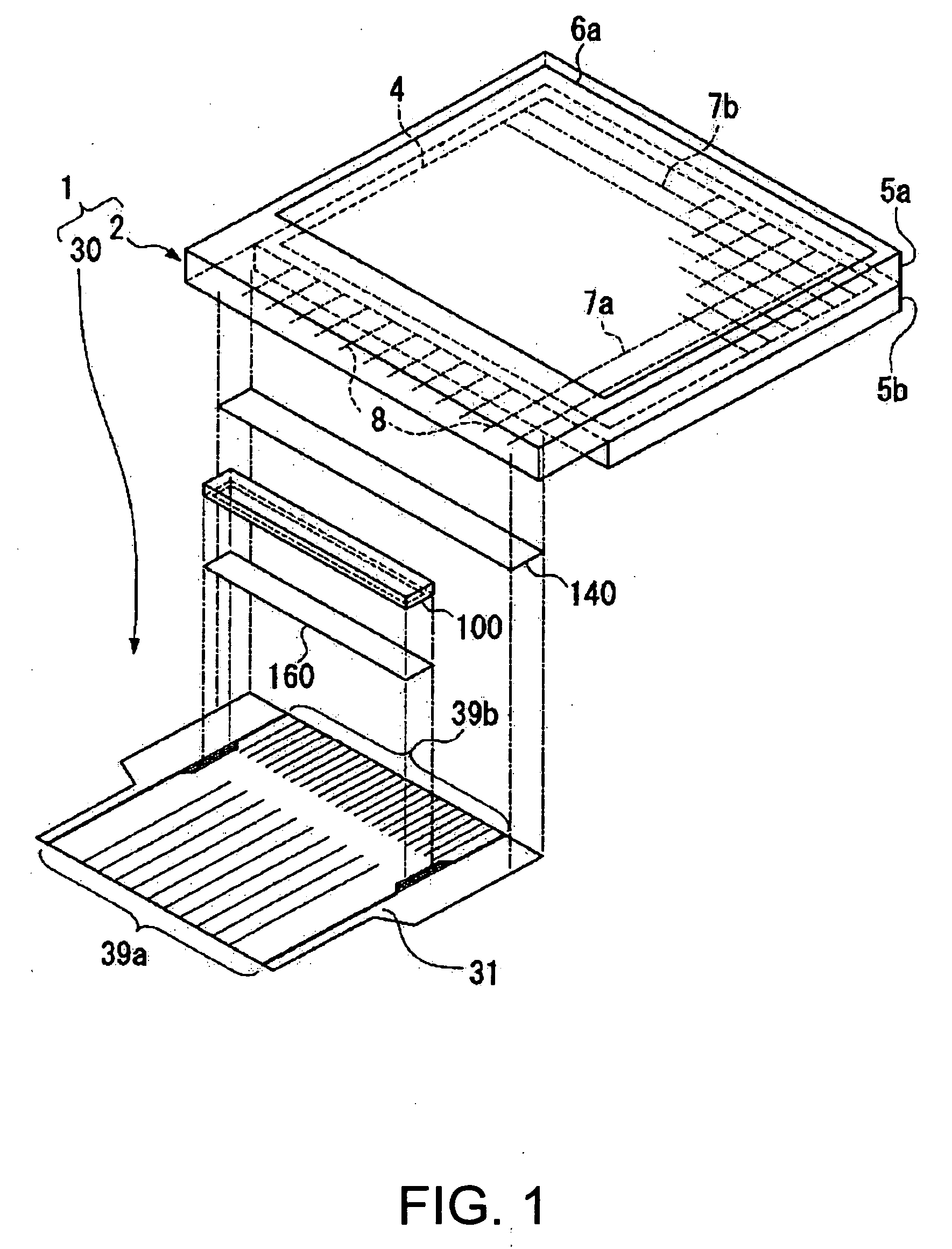
[0047]FIG. 1 is an exploded perspective view of a liquid crystal module with the structure of chip on film (COF). In the present embodiment, a wiring pattern formation method on a flexible printed circuit board (hereinafter, referred to as a FPC) 30 is taken as an example and described. The FPC 30 has electrical wiring patterns 39a and 39b formed on the surface of a film substrate 31 having flexibility. Although the details will be described later, in a liquid crystal module 1 shown in FIG. 1, the FPC 30 is connected to an end of the liquid crystal panel 2 and a liquid crystal drive IC 100 is mounted on the surface of the FPC 30. From this liquid crystal drive IC 100, a drive signal is output through the FPC 30 to the liquid crystal panel 2, thereby displaying an image on the liquid crystal panel 2.
[Wiring Pattern]
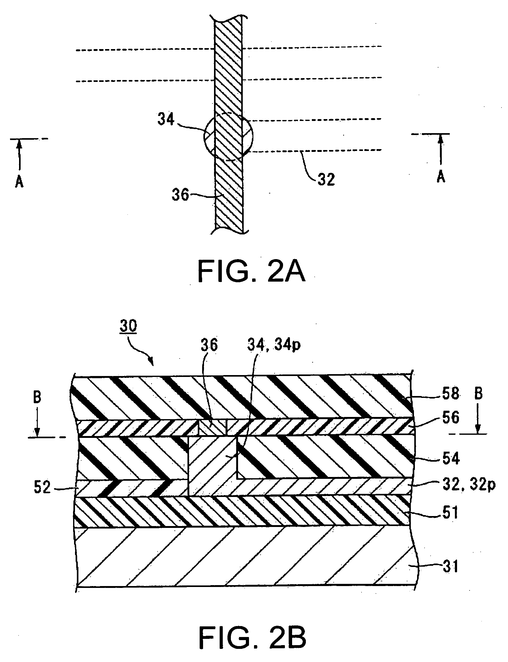
[0048]FIGS. 2A and 2B are explanatory views of a wiring pattern according to the present embodiment and enlarged views of a portion in which the wiring of the FPC is for...
second embodiment
[0106]FIG. 6 is a process table of a wiring pattern formation method according to the second embodiment. FIGS. 7A to 8B are explanatory views of the wiring pattern formation method according to the second embodiment. The processes will be described below in the order of step numbers in the leftmost column of FIG. 6. The processes in steps 1 to 6 and steps 11 to 16 are the same as in the first embodiment and the description thereof will be omitted. Initially, as shown in FIG. 7A, the substrate dielectric film 51 is formed on the surface of the substrate dielectric film 51.
[0107] As shown in FIG. 7B, the liquid lien 32p that will later be an electrical wiring is written and formed on the surface of the substrate dielectric film 51 (step 7a). This writing is performed by the droplet discharge method using the droplet discharge device described later. What is discharged at this point is a dispersion liquid in which conductive fine particles, which is a material for forming the electric...
PUM
| Property | Measurement | Unit |
|---|---|---|
| Volume | aaaaa | aaaaa |
| Ratio | aaaaa | aaaaa |
Abstract
Description
Claims
Application Information
 - R&D
- Intellectual Property
- Life Sciences
- Materials
- Tech Scout
- Unparalleled Data Quality
- Higher Quality Content
- 60% Fewer Hallucinations
Browse by: Latest US Patents, China's latest patents, Technical Efficacy Thesaurus, Application Domain, Technology Topic, Popular Technical Reports.
© 2025 PatSnap. All rights reserved.Legal|Privacy policy|Modern Slavery Act Transparency Statement|Sitemap|About US| Contact US: help@patsnap.com