Hybrid memory device and method for manufacturing the same

a memory device and hybrid technology, applied in the direction of semiconductor devices, basic electric elements, electrical apparatus, etc., can solve the problems of deterioration of the polarization characteristics of the ferroelectric layer, breakdown of the gate oxide layer of the electrically, and the function of logic circuit devices such as memory cell control, etc., to achieve the effect of reducing reducing the initial characteristics of the ferroelectric memory cell array, and eliminating the deterioration of electrical characteristics

Inactive Publication Date: 2006-03-30
LAPIS SEMICON CO LTD
View PDF8 Cites 5 Cited by
  • Summary
  • Abstract
  • Description
  • Claims
  • Application Information

AI Technical Summary

Benefits of technology

[0033] The present invention has been made in consideration of the above-described problems in the related art. It is, therefore, an object of the present invention to provide a ferroelectric memory cell array with excellent electrical characteristics at the time of shipping and higher performance and a hybrid memory device including a logic circuit without deterioration of electrical characteristics.

Problems solved by technology

This reduction reaction leads to deterioration in the polarization characteristics of the ferroelectric layer.
It is possible for this to result in breakdown of the gate oxide layer of the electrically connected transistor through the buried contacts connected to the metal wiring or the like.
That is, if the gate oxide layer becomes like that, for example, the function of the logic circuit device such as memory cell control is broken; and further; the ferroelectric memory malfunctions.
Therefore, particularly, the breakdown of the gate insulating layer of the transistor due to the charge-up phenomena occurs easily in the logic circuit region.
As described above, moisture is unavoidably trapped in the layer formed by the CVD method.
In addition, there is a problem that the characteristics of ferroelectric layer are deteriorated.

Method used


Image

  • Hybrid memory device and method for manufacturing the same
  • Hybrid memory device and method for manufacturing the same
  • Hybrid memory device and method for manufacturing the same

Examples


first embodiment

Construction of the Hybrid Memory Device

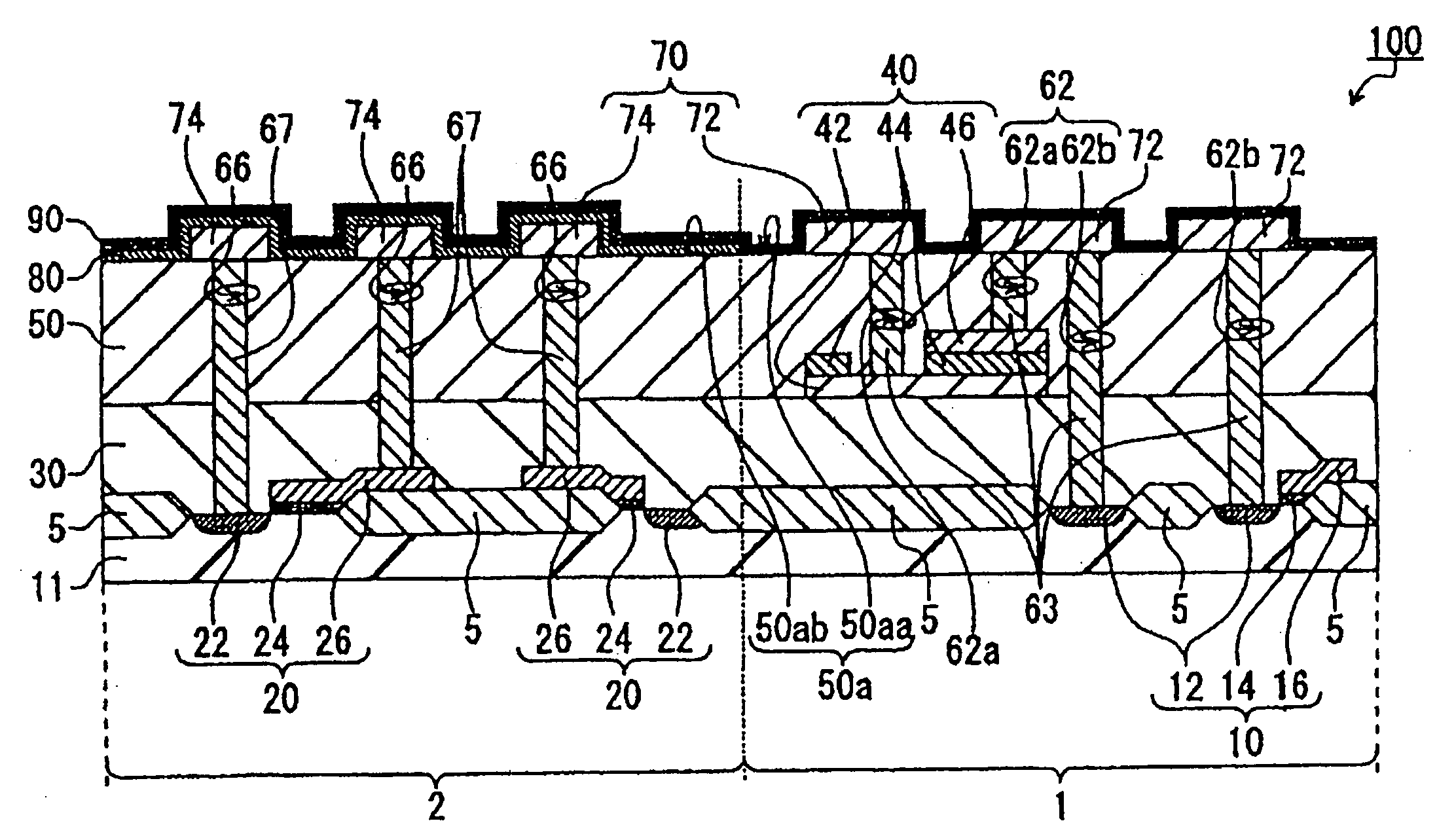
[0064] Referring to FIGS. 2A and 2B, one example of a hybrid memory device of the present invention will be described.

[0065]FIG. 2A is a schematic top view explaining elements of an example of a hybrid memory device in accordance with a first embodiment of the present invention. FIG. 2B is a schematic view representing a cross-section taken along dash dotted line A-A′ of FIG. 2A.

[0066] The hybrid memory device 100 has a feature in a construction of a following liner oxide layer. As for other elements, any suitable elements of a conventional hybrid memory device or a Ferroelectric. Random Access Memory (hereinafter referred to as FeRAM) may be appropriately selected and applied to the present invention.

[0067] As shown in FIGS. 2A and 2B, the hybrid memory device 100 of the present invention takes the form of a chip. In this embodiment, the hybrid memory device 100 has a hexahedral shape.

[0068] As shown in FIG. 2A, the hybrid memory device...

second embodiment

Construction of the Hybrid Memory Device

[0129] Referring to FIG. 4, one example of a hybrid memory device of the present invention will be described.

[0130]FIG. 4A is a schematic top view explaining elements of an example of the present hybrid memory device. FIG. 4B is a schematic view representing a cross-section taken along dash dotted line A-A′ of FIG. 4A.

[0131] The hybrid memory device 100 is characterized in that it includes an offset oxide layer 81 formed on the first wiring unit 72. As for the other elements, since they are similar to those of the first embodiment, a detailed explanation thereof is omitted.

[0132] As shown in FIGS. 4A and 4B, the hybrid memory device 100 in accordance with a second embodiment of the present invention is a type of so-called (semiconductor) chip.

[0133] The hybrid memory device 100 is provided with a semiconductor substrate 11. In the semiconductor substrate 11, a plurality of regions is defined. Similar to the first embodiment, a memory cel...


PUM


Abstract

A hybrid memory device includes a plurality of regions including a memory cell array region upon which are formed a plurality of memory cells and a logic circuit region upon which is formed a logic circuit device, and is provided with a liner oxide layer formed on a region covering the logic circuit region except the memory cell array region and a cover layer formed on the liner oxide layer while extending to the memory cell array region.

Description

BACKGROUND OF THE INVENTION [0001] 1. Field of the Invention [0002] The present invention relates to a hybrid memory device provided with a memory cell to store binary data as a polarization state of a ferroelectric layer and a method for manufacturing the same. [0003] 2. Description of Related Arts [0004] Ferroelectric Random Access Memory (hereinafter referred to as FeRAM) is a representative form of ferroelectric memory. [0005] Recently, as so-called SOC (system on chip) technology has been developed, a hybrid memory device having a structure provided with functions different from those of FeRAM cells, i.e., integrating a logic circuit to perform processes related to the FeRAM cells and an RF circuit or the like into one chip, has been introduced (see pages 1 12-125 of NEW DEVELOPMENT OF FeRAM, CMC Publication). [0006] A ferroelectric layer incorporated into the above-described FeRAM is formed of an oxygen compound material. The oxygen compound material is reduced by hydrogen (H2...

Claims


Application Information

Patent Timeline
Patent Type & Authority Applications(United States)
IPC IPC(8): H01L29/94
CPCH01L21/76834H01L27/11507H01L27/11502H01L21/76838H10B53/30H10B53/00
Inventor KAJITA, YOKOKOIWA, ICHIROKANEHARA, TAKAOASHIKAGA, KINYAABE, KAZUHIDE
Owner LAPIS SEMICON CO LTD
Why Eureka
Try Eureka