
Versatile system for time-independent signal sampling

a time-independent, signal sampling technology, applied in the direction of digital variable/waveform display, analog circuit testing, instruments, etc., can solve the problems of high-performance semiconductor devices that strain or exceed the functional limits of automated test equipment (ate) utilized in many commercial semiconductor production processes, and the parametric performance level of certain ate functions is limited or fixed at legacy values, etc., to achieve accurate and stable signal sampling, easy to use, efficient and cost-effective

Inactive Publication Date: 2006-03-23
TEXAS INSTR INC
View PDF5 Cites 8 Cited by
  • Summary
  • Abstract
  • Description
  • Claims
  • Application Information

AI Technical Summary

Benefits of technology

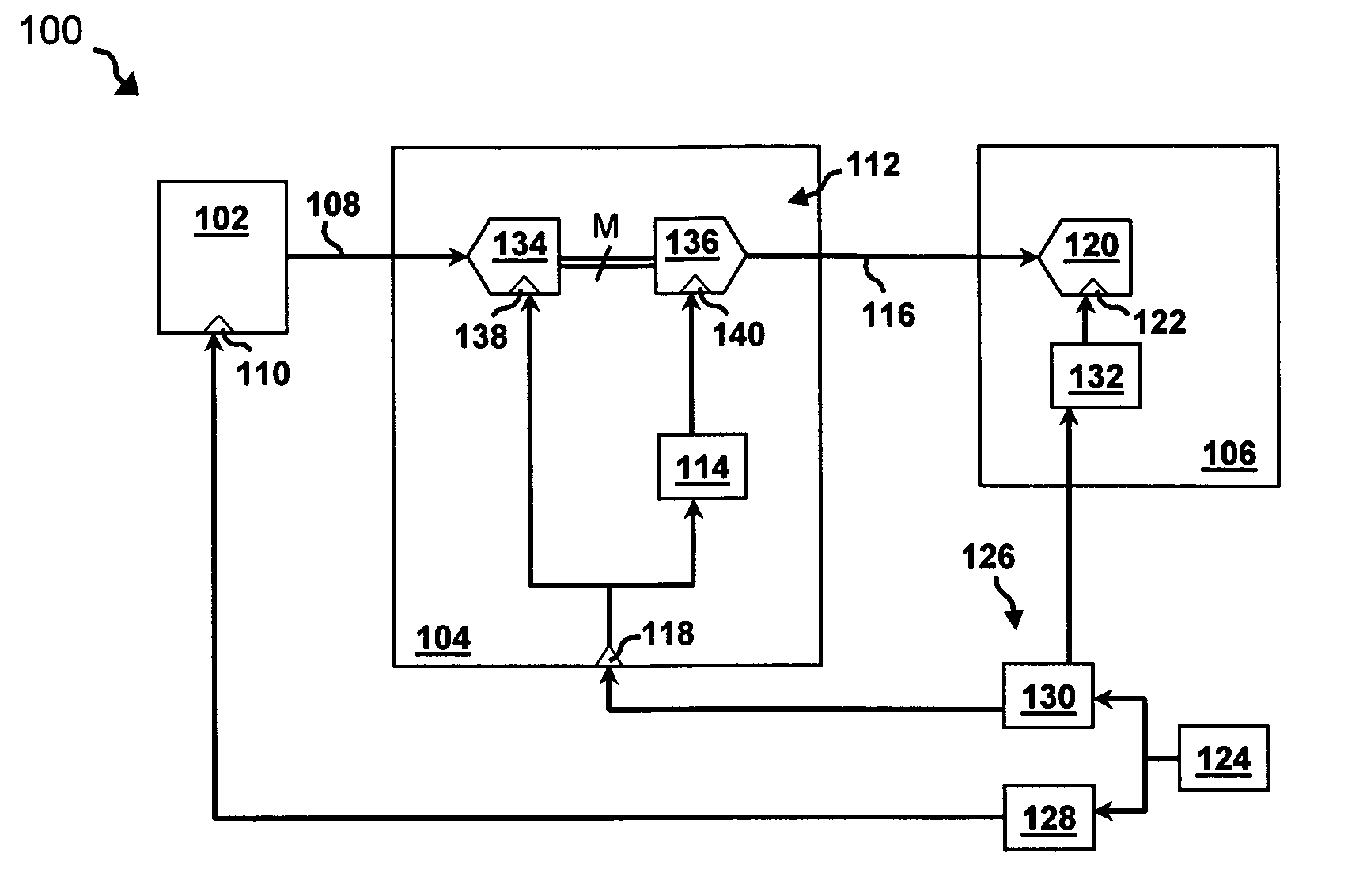
[0010] The present invention provides a versatile system, comprising a number of apparatus and methods, for accurate and stable signal sampling that overcomes incongruities between signal rate capabilities of DUTs and ATE. The system of the present invention obviates instabilities due to capacitive signal dissipation—providing time-independent signal sampling. The system of the present invention utilizes commercially viable components that are readily adaptable to a number of design and fabrication processes—overcoming certain limitations associated with conventional approaches in an easy, efficient and cost-effective manner.
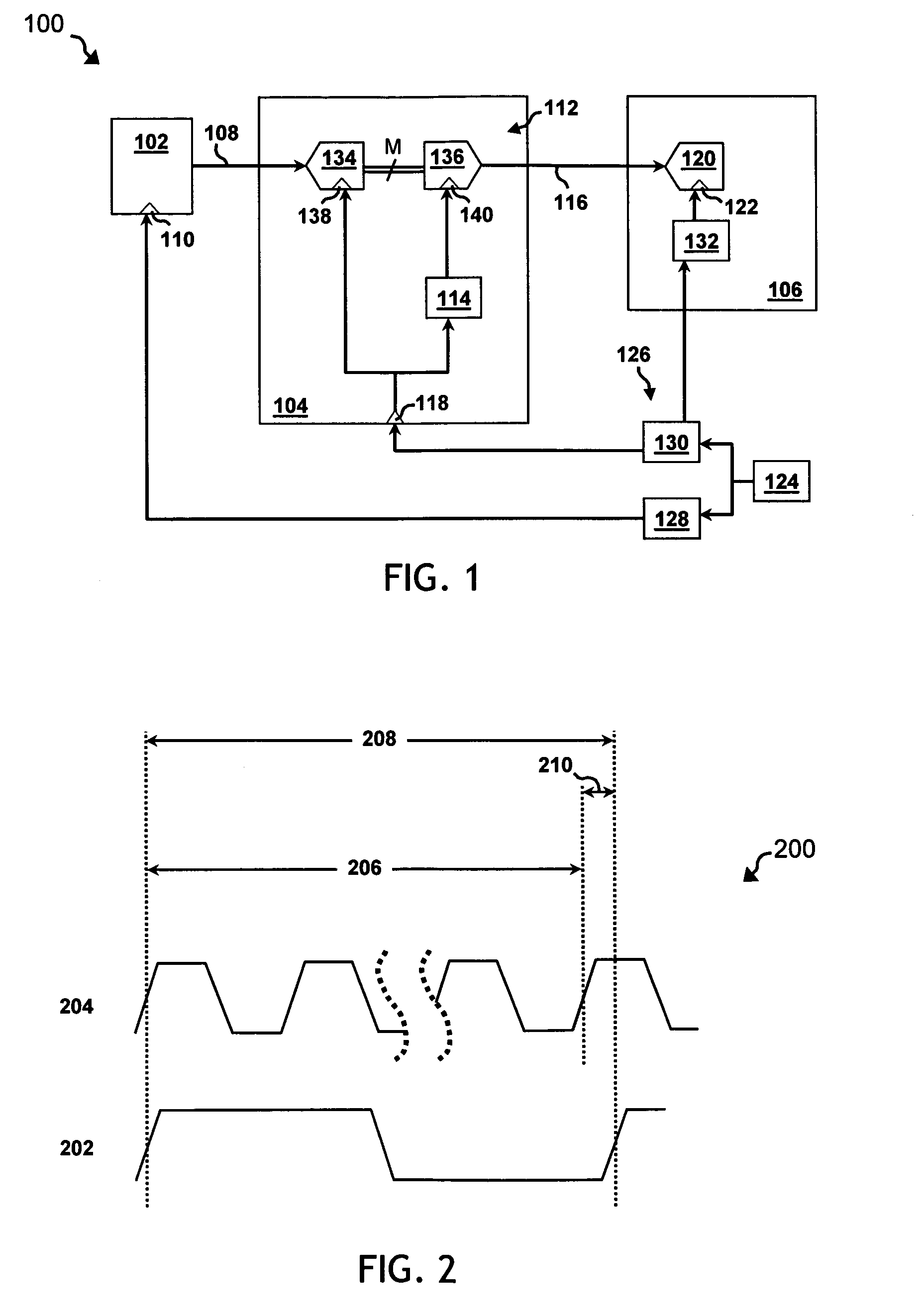
[0011] Specifically, the system of the present invention provides analog-to-analog sampling, using analog-to-digital-to-analog (A / D / A) conversion. The system of the present invention further provides sample decimation. The system of the present invention applies A / D / A conversion in conjunction with sample decimation to analyze or sample a desired test signal. The A / D / A conversion of the present invention provides a stable, discrete sample value that may be held indefinitely without degradation. The sample decimation of the present invention provides a desired sampling resolution and performance optimization, regardless of a desired test signal's period length. The system of the present invention thus provides test signal sampling of a desired resolution that is time-independent—obviating performance incongruities between an advanced DUT and an ATE system.

Problems solved by technology

The continual demand for enhanced performance in electronic devices—particularly with respect to integrated circuits operating therein—has resulted in dramatic alterations of semiconductor device properties and behaviors.
The increasing circuit density and performance levels of such cutting-edge devices generate a number of challenges to commercial semiconductor manufacturing processes.
For example, high-density, high-performance semiconductor devices often strain or exceed the functional limits of automated test equipment (ATE) utilized in many commercial semiconductor production processes.
As such, parametric performance levels (e.g., signal frequency) of certain ATE functions are limited or fixed at legacy values.
For certain testing needs, this basic disconnect between tester performance and the performance of a device under test (DUT) can cause a number of testing irregularities or errors.
Consider, for example, issues that arise in testing devices that implement high-speed serial interface protocols (e.g., Ethernet, USB).
Unfortunately, even the newest and most advanced ATE often lacks the degree of resolution necessary to reliably test at such advanced performance levels.
Unfortunately, even advanced ATE systems often lack the necessary bandwidth to successfully test at such levels.
Such incongruities between DUT and ATE performance levels can significantly impact the progress or efficiency of device testing or characterization.
Accurate test data, if even obtainable, may take a long time to compile.
More daunting problems may arise from erroneous data introduced into device testing or characterization.
The ATE may therefore not be able to accurately assess boundaries of the 2 ns window—whether only a portion, or all, of the 2 ns window is subsumed within a given 4 ns window.
As a result, pass or fail data for the device may have an unusually high probability of error—potentially decreasing device yield or increasing the likelihood of end-equipment failures.
Although conventional sample and hold schemes are somewhat helpful in this regard, they also introduce certain performance issues that require designers to make a number of tradeoffs.
Due to their precision, however, these devices tend to be relatively expensive and of limited usefulness for commercial ATE systems.
Unfortunately, such small capacitors have relatively high droop rates—i.e., signal charges stored thereon begin to dissipate severely and rapidly.
Severe droop rates limit the usefulness of such devices in ATE applications requiring extended signal evaluation.
Although these devices tend to have lower droop rates than high-performance versions, they are typically still not robust enough for extended signal evaluation.
They generally lack the resolution or retention necessary for full and accurate testing in high-performance applications.

Method used


Image

  • Versatile system for time-independent signal sampling
  • Versatile system for time-independent signal sampling

Examples


Embodiment Construction

[0019] While the making and using of various embodiments of the present invention are discussed in detail below, it should be appreciated that the present invention provides many applicable inventive concepts, which can be embodied in a wide variety of specific contexts. The present invention is hereafter illustratively described in conjunction with the automated testing of high signal edge-rate device technologies. The specific embodiments discussed herein are, however, merely demonstrative of specific ways to make and use the invention and do not limit the scope of the invention.

[0020] The present invention comprehends a number of issues arising in certain conventional ATE testing applications. Typically, ATE utilized in commercial semiconductor manufacturing processes lacks instrumentation capable of directly capturing or characterizing a number of high-speed signals. Generally, such ATE systems receive—as an input—a signal transmitted from a DUT. Certain problems arise when the...


PUM


Abstract

The present invention provides a system (100) that overcomes performance incongruities between a high-speed device (102) and commercial ATE (106). The system of the present invention provides an analog-to-analog sampler (104), having a clock input (118). The analog-to-analog sampler receives a first analog test signal (108) from the high-speed device, and converts it into a second analog test signal (116) at a desired rate, utilizing an analog-to-digital-to-analog conversion function (112) and a decimation function (114). The ATE system houses an analog capture component (120). The analog capture component has a clock input (122), and receives the second analog test signal for conversion into digital format. A series of clock signals (126) are generated from a common frequency reference source (124), to provide the necessary clock signals throughout the system.

Description

TECHNICAL FIELD OF THE INVENTION [0001] The present invention relates generally to the field of automated semiconductor device testing and, more particularly, to apparatus and methods for reliably sampling high edge rate analog test signals in a time-independent manner. BACKGROUND OF THE INVENTION [0002] The continual demand for enhanced performance in electronic devices—particularly with respect to integrated circuits operating therein—has resulted in dramatic alterations of semiconductor device properties and behaviors. Efforts are continually made to reduce the size of most substructures within semiconductor devices, even while performance demands on those devices are continually increased. A number of improvements and innovations in fabrication processing, material composition, and layout of the active circuit levels of a semiconductor device have resulted in very high-density circuit designs that operate at very high performance levels. The increasing circuit density and perfor...

Claims


Application Information

Patent Timeline
Patent Type & Authority Applications(United States)
IPC IPC(8): G01R13/02
CPCG01R19/2509G01R31/316G01R31/2834
Inventor GUIDRY, DAVID W.
Owner TEXAS INSTR INC
Learn More