Light scanning device

a scanning device and light technology, applied in the field of light scanning devices, can solve the problems synchronous timing deviation, and inability to support synchronous timing deviation, so as to reduce or eliminate the deviation of synchronous timing, reduce or eliminate the effect of synchronous timing deviation

Active Publication Date: 2006-03-16
HOYA CORP
View PDF3 Cites 0 Cited by
  • Summary
  • Abstract
  • Description
  • Claims
  • Application Information

AI Technical Summary

Benefits of technology

[0007] The present invention is advantageous in that an improved light scanning device includes a synchronizing signal generating circuit. The synchronizing signal generating circuit is configured to reduce or eliminate the deviation of synchronous timing in spite of the DC level shift, which depends on a power supply voltage and / or temperature. The synchronizing signal generating circuit is also configured to reduce or eliminate the deviation of synchronous timing in spite of the level fluctuation of a light receiving signal outputted from a PD.

Problems solved by technology

In such a technology, there is a problem that when fluctuations occur in the level of the light receiving current Io outputted from the PD 5 and / or the DC level (dark current, offset current) of the I-V converting circuit 11 that converts the light receiving current to the light receiving voltage Vo, the waveform of the SOS signal is deformed to cause timing deviation (phase shift in time domain) of the SOS signal.
Similarly in this case, the fluctuation of the pulse width of the SOS signal results in the deviation of the synchronous timing.
However, it cannot support the deviation of the synchronous timing that is caused by uncertain factors such as the level fluctuation of the PD output depending on temperature and / or time and the DC level shift of the I-V converting circuit.

Method used


Image

  • Light scanning device
  • Light scanning device
  • Light scanning device

Examples


first embodiment

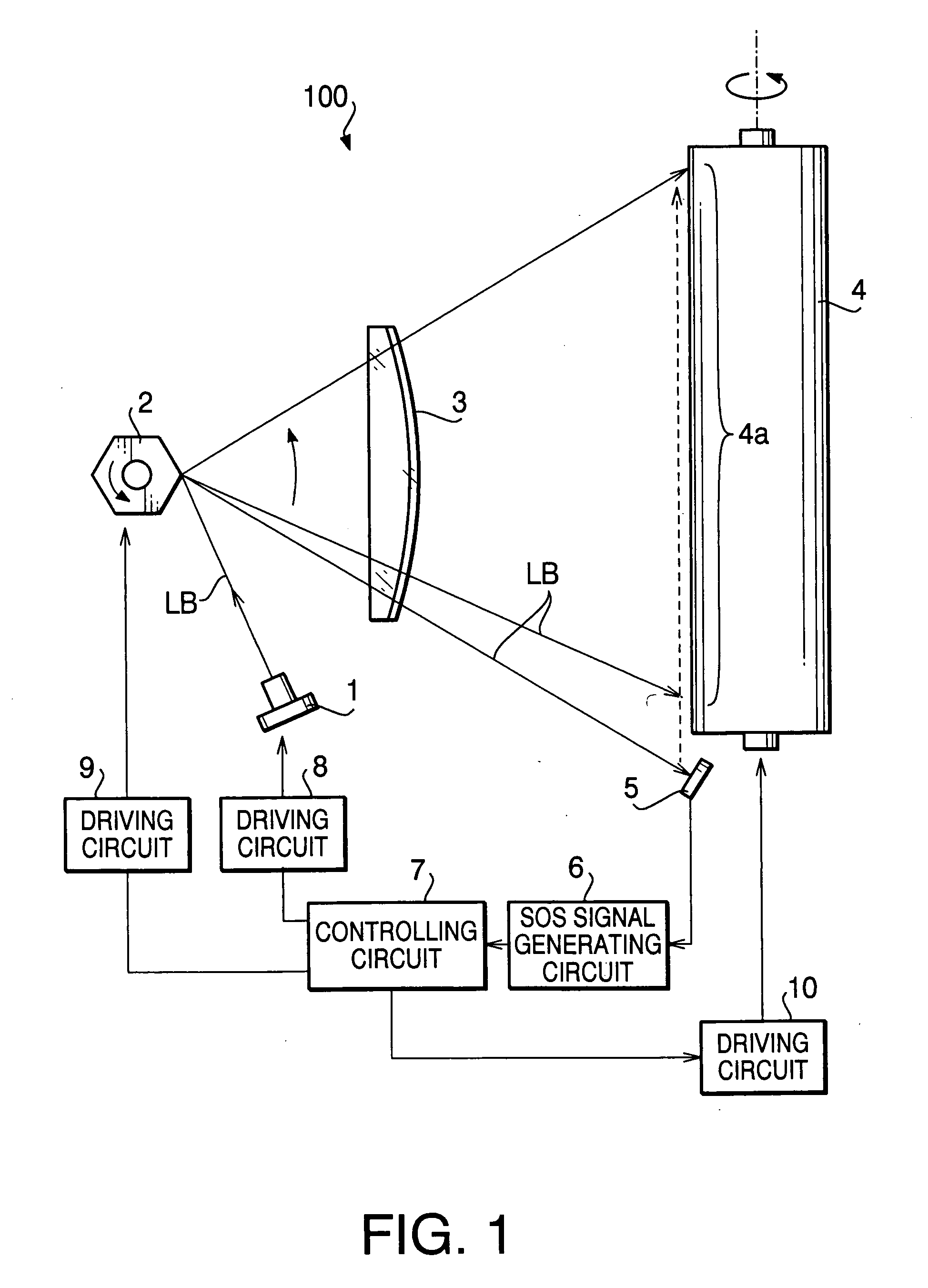
[0031] Next, a first embodiment of the present invention will be described with reference to the accompanying drawings. In a laser scanning device 100 shown in FIG. 1, to which the first embodiment is applied, an SOS signal is generated by an SOS signal generating circuit 6 on the basis of a light receiving signal outputted from a PD 5 while receiving a laser beam, and is inputted to a controlling circuit 7. The controlling circuit 7, based on the inputted SOS signal, controls an LD driving circuit 8 to control emission from an LD 1, and controls a polygon mirror driving circuit 9 and a photoconductive drum driving circuit 10. Thereby, the laser beam is scanned on a predetermined area 4a of the photoconductive drum 4 in synchronization with the SOS signal to draw a required pattern.

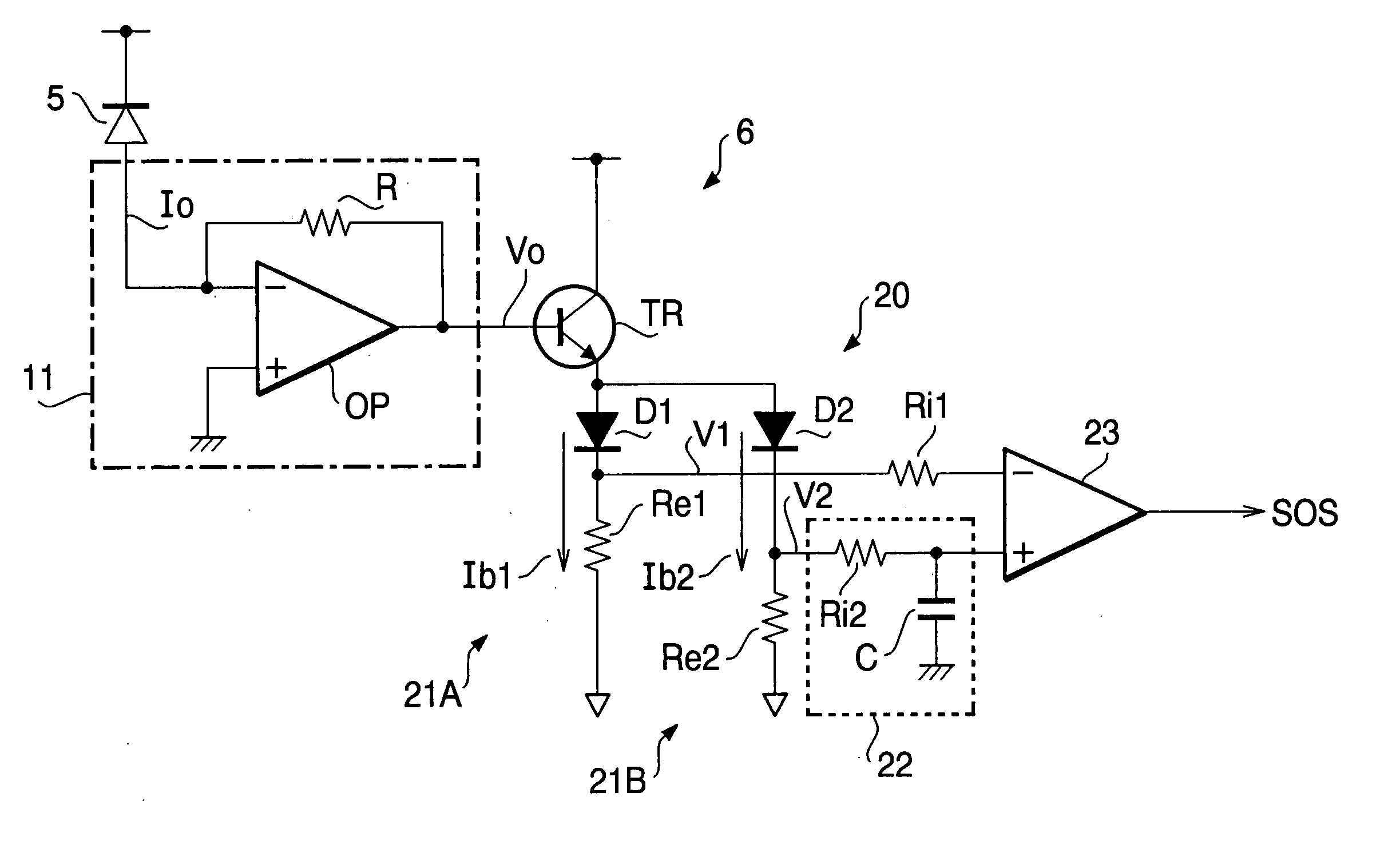
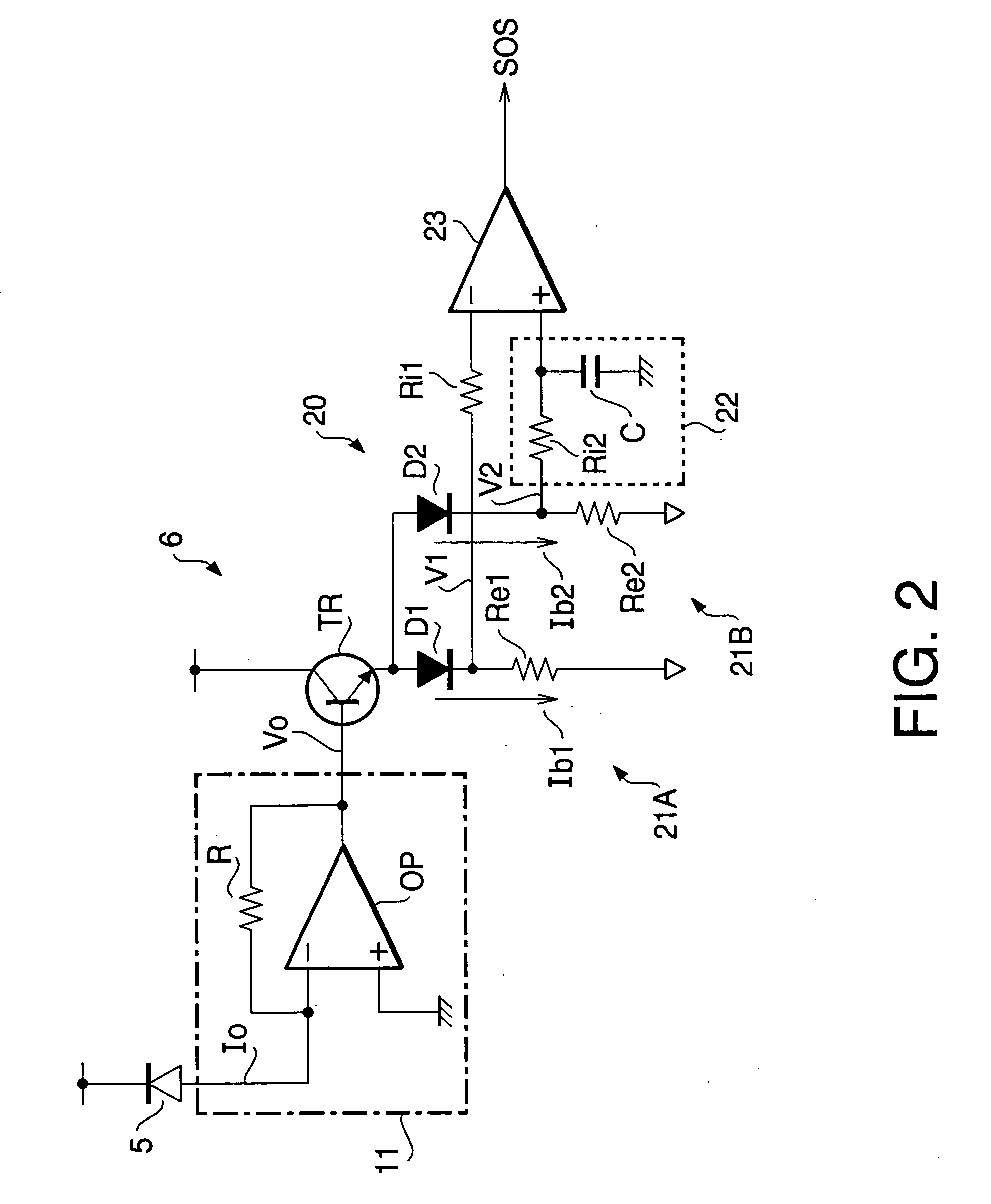
[0032]FIG. 2 is a circuit diagram of the SOS signal generating circuit 6. The SOS signal generating circuit 6 is configured with an SOS signal detecting circuit 20 and with an I-V converting circuit 11 t...

second embodiment

[0042]FIG. 6 is a circuit diagram of an SOS signal generating circuit of a second embodiment according to the present invention, in which the same reference numbers are assigned to parts equivalent to the first embodiment. The second embodiment is different from the first embodiment in configurations of first and second bias superimposing circuits 21A and 21B of an SOS signal detecting circuit 20. The first and second bias superimposing circuits 21A and 21B are configured with first and second NPN transistors TR1 and TR2 with the same specifications, respectively. In the first bias superimposing circuit 21A, a light receiving voltage outputted from an I-V converting circuit 11 is applied to the base of the first NPN transistor TR1 via a first base resistor Rb1, while the light receiving voltage, in the second bias superimposing circuit 21B, is applied to the base of the second NPN transistor TR2 via a second base resistor Rb2 with the same resistance as the first base resistor Rb1. ...

third embodiment

[0044]FIG. 7 is a circuit diagram of an SOS signal generating circuit of a third embodiment. The configurations of first and second bias superimposing circuits 21A and 21B in the third embodiment are the same as that of the second embodiment. That is to say, the first and second bias superimposing circuits 21A and 21B are configured with NPN transistors TR1 and TR2 with the same specification, respectively, and in the first bias superimposing circuit 21A, a light receiving voltage Vo outputted from an I-V converting circuit 11 is applied to the base of the first NPN transistor TR1 via a first base resistor Rb1, while the light receiving voltage Vo, in the second bias superimposing circuit 21B, is applied to the base of the second NPN transistor TR2 via a second base resistor Rb2 with the same resistance as the first base resistor Rb1. The emitters of the first and second NPN transistors TR1 and TR2 are connected with the first and second emitter resistors Re1 and Re2, respectively, ...


PUM


Abstract

A light scanning device capable of scanning a light beam on a photosensitive surface includes a light receiving system configured to receive the light beam and output a light receiving signal and a synchronizing signal generating system configured to generate a synchronizing signal with which light scanning is synchronized. The synchronizing signal generating system includes a first bias superimposing system configured to superimpose a first bias signal onto the light receiving signals to generate a first light receiving signal, a second bias superimposing system configured to superimpose a second bias signal with a different level from that of the first bias signal onto the light receiving signals to generate a second light receiving signal, a waveform shaping system configured to shape the waveform of the second light receiving signal, and a comparing system configured to compare the first light receiving signal with the second light receiving signal to output the synchronizing signal.

Description

BACKGROUND OF THE INVENTION [0001] The present invention relates to a light scanning device used for a laser beam printer, etc. More particularly, the present invention relates to a laser scanning device, and especially to a circuit configured to detect an SOS (start-of-scan) signal used as a synchronizing signal for determining laser scanning timing. [0002] So as to obtain an SOS signal used as a timing signal while scanning a laser beam on a image plane, a laser scanning device is configured to generate the SOS signal based on a light receiving signal outputted from a photo diode (hereinafter, referred to as a PD) that receives the scanned laser beam. For instance, in a laser scanning device as indicated in FIG. 1, a laser beam LB emitted from a laser diode (hereinafter, referred to as an LD) 1 is deflected and scanned by a rapidly rotating polygon mirror 2 within a predetermined angle range, and main scanning of the LB directed to a photoconductive drum 4 through an fθ lens 3 is ...

Claims


Application Information

Patent Timeline
Patent Type & Authority Applications(United States)
IPC IPC(8): H01J40/14H01J3/14G03G15/01
CPCG06K15/1219H04N1/053H04N1/1135H04N1/12H04N2201/0471H04N2201/04732H04N2201/04744
Inventor MINAKUCHI, TADASHI
Owner HOYA CORP
Why Eureka
Try Eureka