
Organic electroluminescence element

a technology of electroluminescence element and organic el, which is applied in the direction of luminescent compositions, organic semiconductor devices, tubes with screens, etc., can solve the problems of inconvenient long luminescent wavelengths, high driving voltage insufficient efficiency and etc., to achieve the effect of improving the durability of organic el elements

Inactive Publication Date: 2006-03-16
IDEMITSU KOSAN CO LTD
View PDF11 Cites 29 Cited by
  • Summary
  • Abstract
  • Description
  • Claims
  • Application Information

AI Technical Summary

Benefits of technology

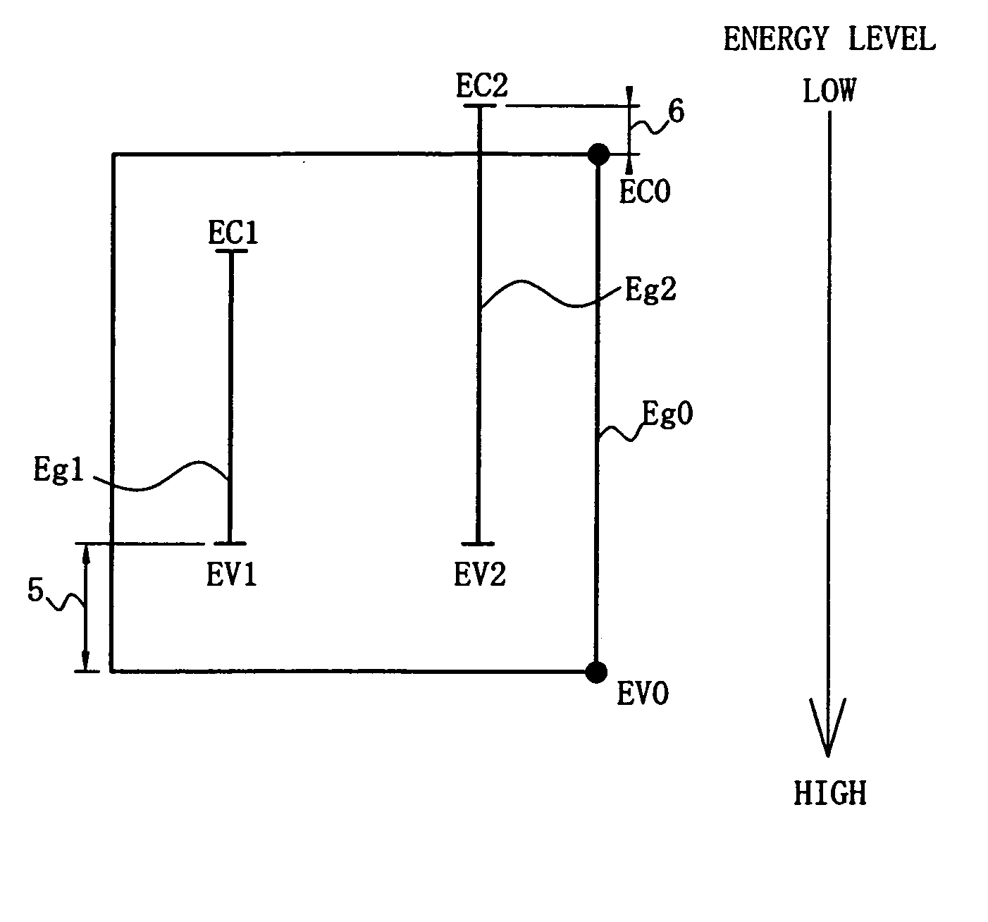
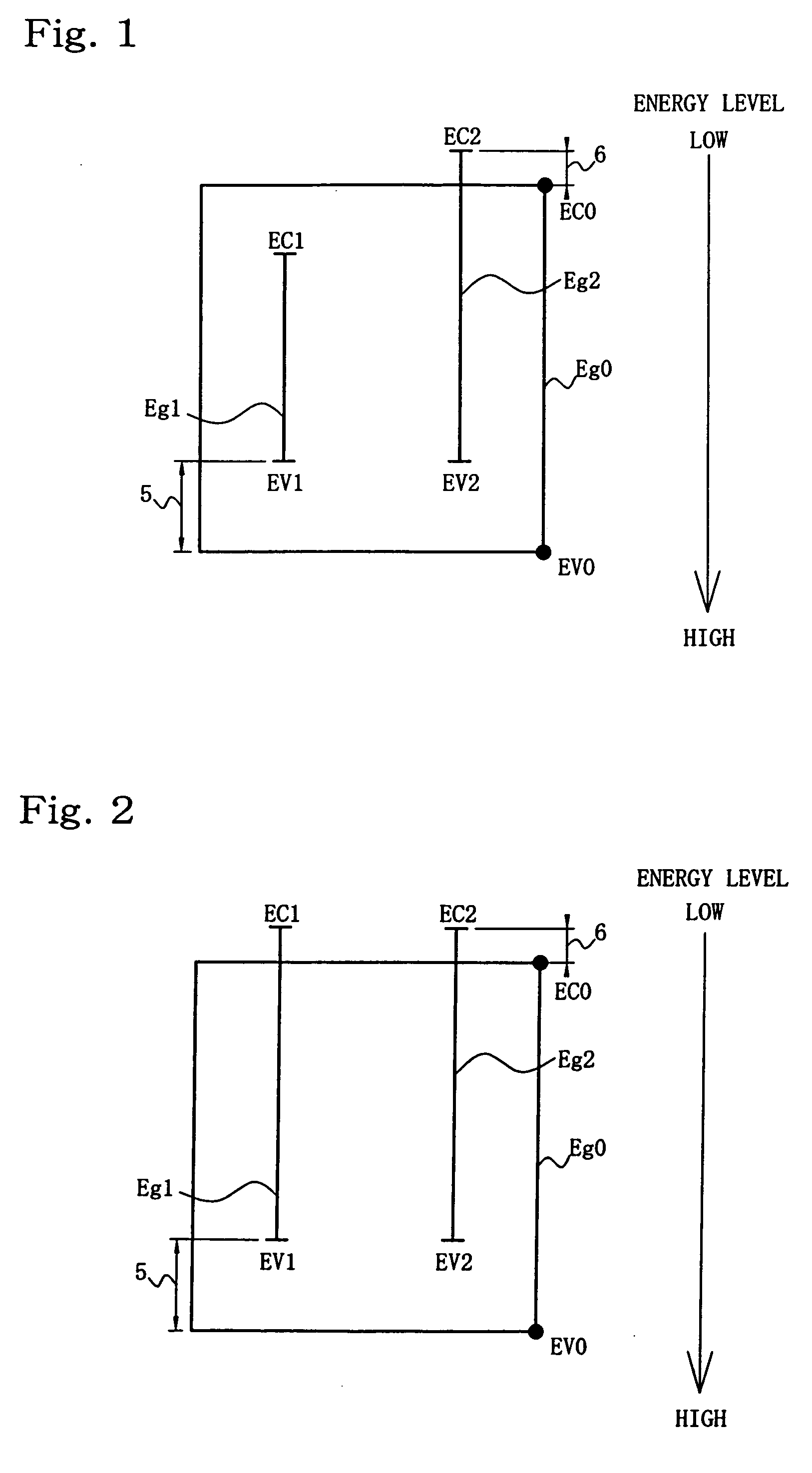
[0029] The inventors have made various researches about dopants, and found out that light can be emitted even if the conduction level of a dopant is lower than the conduction level of a host. Furthermore, the inventors have found out that on the basis of this fact, the durability of an organic EL element is improved when energy gaps of a host and a dopant therein satisfy a specific relation, and then made the present invention.

Problems solved by technology

However, an organic EL element having a sufficient efficiency and durability has not been developed.
In this technique, however, the light emitting layer captures both kinds of charges of holes and electrons by using a single luminescent dopant; therefore, the luminescent wavelength therefrom is inconveniently long.
When the addition concentration thereof is increased to sufficiently obtain the advantageous effect of the dopant, the electron trapping property becomes stronger so as to cause a problem that the driving voltage of the organic EL element becomes high.
Further, when the addition concentration becomes larger, the molecules of the dopant contact each other, thereby causing concentration quenching to result in a problem that the efficiency of the organic EL element becomes low.
However, the effect of improving the emission lifetime is small.

Method used


Image

  • Organic electroluminescence element
  • Organic electroluminescence element
  • Organic electroluminescence element

Examples


example 1

[0162] A grass substrate of 25 mm by 75 mm by 1.1 mm with an ITO transparence electrode (GEOMATEC CO., LTD.) was subjected to ultrasonic cleaning with isopropyl alcohol for 5 minutes, and cleaned with ultraviolet rays and ozone for 30 minutes.

[0163] The resultant substrate was mounted on a substrate holder in a vacuum deposition device. First, a film of N,N′-bis(N,N′-diphenyl-4-aminophenyl)-N,N′-diphenyl-4,4′-diamino-1,1′-biphenyl (TPD232 film), having a film thickness of 60 nm, was formed so as to cover the surface of the transparence electrode on which transparence electrode lines were formed. The TPD232 film functions as a hole injecting layer.

[0164] After forming the TPD232 film, a layer of N,N,N′,N′-tetra(4-biphenyl)-diaminobiphenylene (TBDB layer), having a film thickness of 20 nm, was formed on the TPD232 film. The film functions as a hole transporting layer.

[0165] Thereafter H1 as a light-emitting-layer material, D1 as a first dopant and D2 as a second dopant were deposit...

example 2

[0168] An organic EL element was produced in the same way as Example 1 except that H2 was used instead of H1, and D3 was used instead of D1.

example 3

[0169] An organic EL element was produced in the same way as Example 2 except that D1 was used instead of D2.


PUM


Abstract

An organic electroluminescence element comprising: a pair of electrodes, and a light emitting layer provided between the pair of electrodes, the layer comprising a light-emitting-layer material, a first dopant and a second dopant that satisfy the following relations, EV0>EV1 and EV0>EV2  (A) EC0≧EC2  (B) EG0>EG1 and EG0>EG2  (C) wherein EV0, EV1 and EV2 are the valence electron levels of the light-emitting-layer material, the first dopant and the second dopant, respectively; EC0 and EC2 are the conduction levels of the light-emitting-layer material and the second dopant, respectively; and EG0, EG1 and EG2 are the energy gaps of the light-emitting-layer material, the first dopant and the second dopant, respectively.

Description

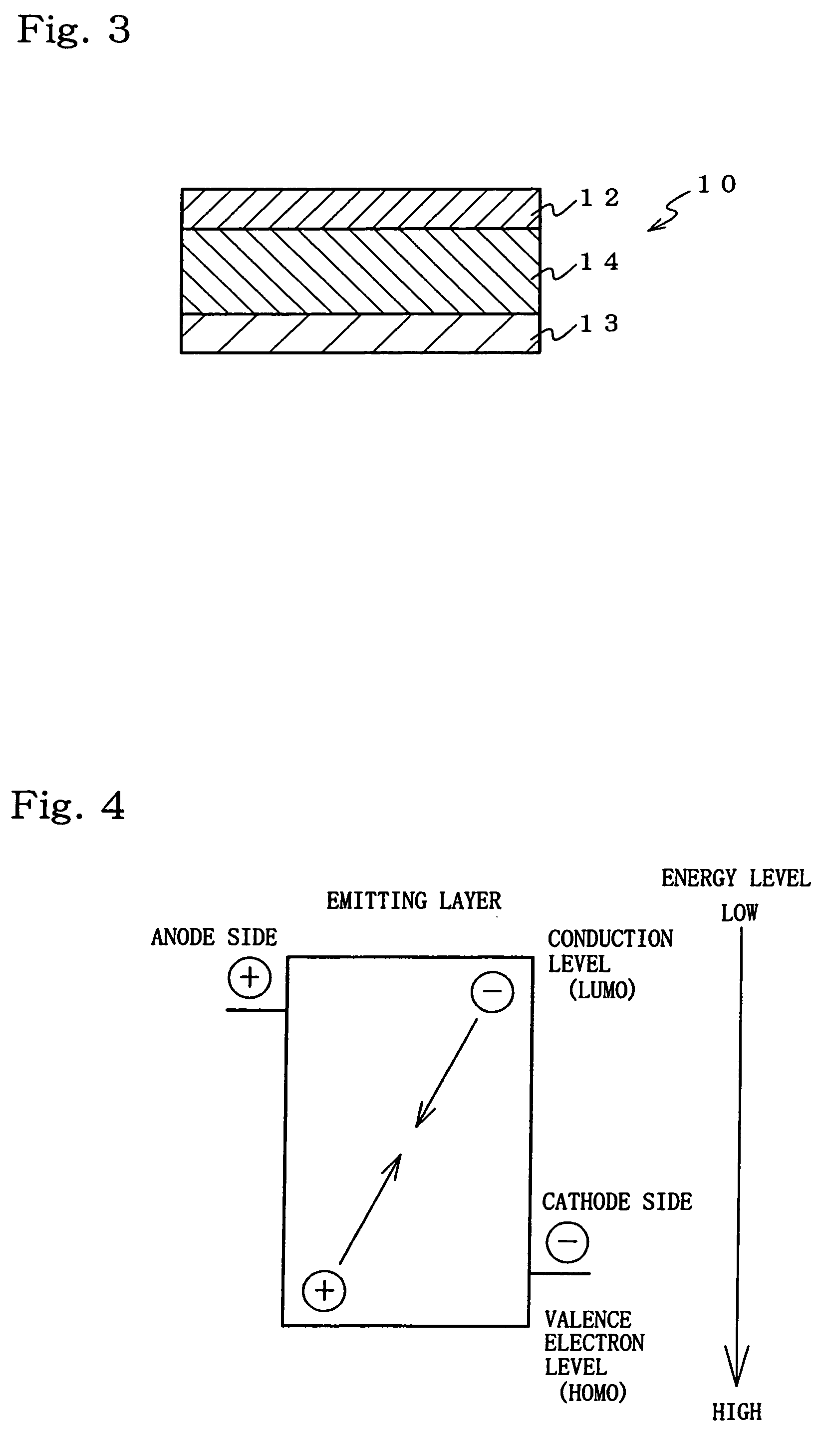
TECHNICAL FIELD [0001] The present invention relates to an organic electroluminescence element. BACKGROUND ART [0002] About organic electroluminescence elements (referred to as organic EL elements hereinafter) using an organic substance, the use thereof as inexpensive, large-area, full color display devices of a solid light emission type, has been promising, and many developments thereof have been made. [0003] An organic EL element is composed of a light emitting layer and a pair of opposite electrodes. FIG. 3 is a sectional view of an ordinary organic EL element. [0004] This organic EL element 10 has a light emitting layer 14 sandwiched between a pair of electrodes, an anode 12 and a cathode 13. The light emitting layer 14 is usually composed of plural laminated layers. When an electric field is applied across the electrodes 12 and 13 in this element 10, electrons are injected from the cathode 13 and holes are injected from the anode 12. The electrons and the holes are recombined i...

Claims


Application Information

Patent Timeline
IPC IPC(8): H01J31/00C09K11/06H01L51/00H01L51/30H01L51/50H05B33/14H05B33/18
CPCC09K11/06H01L51/5004C09K2211/1011C09K2211/1014C09K2211/1088H01L51/005H01L51/0052H01L51/0058H01L51/0059H01L51/007H01L51/0081H01L51/5012H01L51/5036H01L2251/308H05B33/14H05B33/18C09K2211/1007H10K85/60H10K85/6565H10K85/626H10K85/631H10K85/615H10K85/324H10K50/11H10K2101/40H10K50/125H10K2102/103
Inventor FUNAHASHI, MASAKAZUFUKUOKA, KENICHIHOSOKAWA, CHISHIO
Owner IDEMITSU KOSAN CO LTD
Learn More