Photovoltaic module with an electronic device in the laminated stack

a photovoltaic module and laminated stack technology, applied in the field of photovoltaic modules, can solve the problems of limiting the power received by the shaded cell, damage to the laminated stack and the module, and no longer delivering electrical energy, so as to improve the heat dissipation of the bypass diodes and reduce the cost

Inactive Publication Date: 2006-03-16
PHOTOWATT INT
View PDF9 Cites 46 Cited by
  • Summary
  • Abstract
  • Description
  • Claims
  • Application Information

AI Technical Summary

Benefits of technology

[0019] The object of the invention is to remedy the drawbacks set out above by proposing a photovoltaic module in which the heat dissipation of the bypass diodes is improved at lower cost.
[0020] To this end, the invention provides a photovoltaic module comprising one or more photovoltaic cells connected in series and disposed inside a laminated stack of glass and polymer, and an electronic protection device, e.g. a bypass diode, arranged to bypass the electric current passing through at least one photovoltaic cell, the electronic protection device being a semiconductor circuit that is disposed inside the laminated stack, wherein the semiconductor circuit is electrically connected to the cells of the module via at least one flat metal ribbon disposed in the laminated stack in order to dissipate the heat energy given off by the semiconductor circuit.
[0021] This arrangement of the photovoltaic cells and of the bypass diodes in a photovoltaic module enables some of the cabling to be omitted. There is no longer any need for the flat copper ribbons to extend outside the laminated stack in order to protect the photovoltaic module with bypass diodes. The flat metal ribbons serve to improve the heat dissipation of the semiconductor circuit by establishing a large heat exchange area with the surrounding elements and also with the outside of the module.

Problems solved by technology

When one of the photovoltaic cells of the module is shaded, i.e. when it is not receiving light either because of damage or because it has been covered by an opaque material, e.g. a leaf, then the cell no longer delivers any electrical energy.
The power Wo received by the shaded cell that can reach the maximum power produced by all the other cells in the module, such that the shaded cell heats up, which can lead to it being destroyed, and also to damage to the laminated stack and to the module.
As a result, a shaded cell is protected since the bypass diode starts conducting the current, thereby limiting the power received by the shaded cell.
Furthermore, the shaded cell receives only the power delivered by the other photovoltaic cells in the same group of cells protected by the same bypass diode in the module, thereby limiting the extent to which it heats up and reducing the loss of energy from the module.
The smaller the number of cells in a group of cells that is protected by a bypass diode, the greater the extent to which heating is limited and energy losses are small.
The heat dissipated by the bypass diodes in junction boxes may not be sufficient.
The stiffer test criteria lead to an increase in the amount of the heat dissipated by bypass diodes.
In the present state of the art it is not possible to satisfy the new standard without using power bypass diodes or without installing radiators on the bypass diodes, as disclosed in U.S. Pat. No. 6,225,793, thereby considerably increasing the cost of the module.
In addition, putting other semiconductor circuits for monitoring and controlling the module, e.g. circuits of the metal-oxide-silicon field effect transistor (MOSFET), thyristor, or gate turn-off thyristor (GTO) type in the junction boxes increases the complexity of the cabling between a junction box and the photovoltaic cells.
In document WO99 / 62125, the bypass diodes are mounted in the laminated stack on the photovoltaic cells so as the photovoltaic cells dissipate the heat provided by the bypass diode but this dissipation is not enough.

Method used


Image

  • Photovoltaic module with an electronic device in the laminated stack
  • Photovoltaic module with an electronic device in the laminated stack
  • Photovoltaic module with an electronic device in the laminated stack

Examples


Embodiment Construction

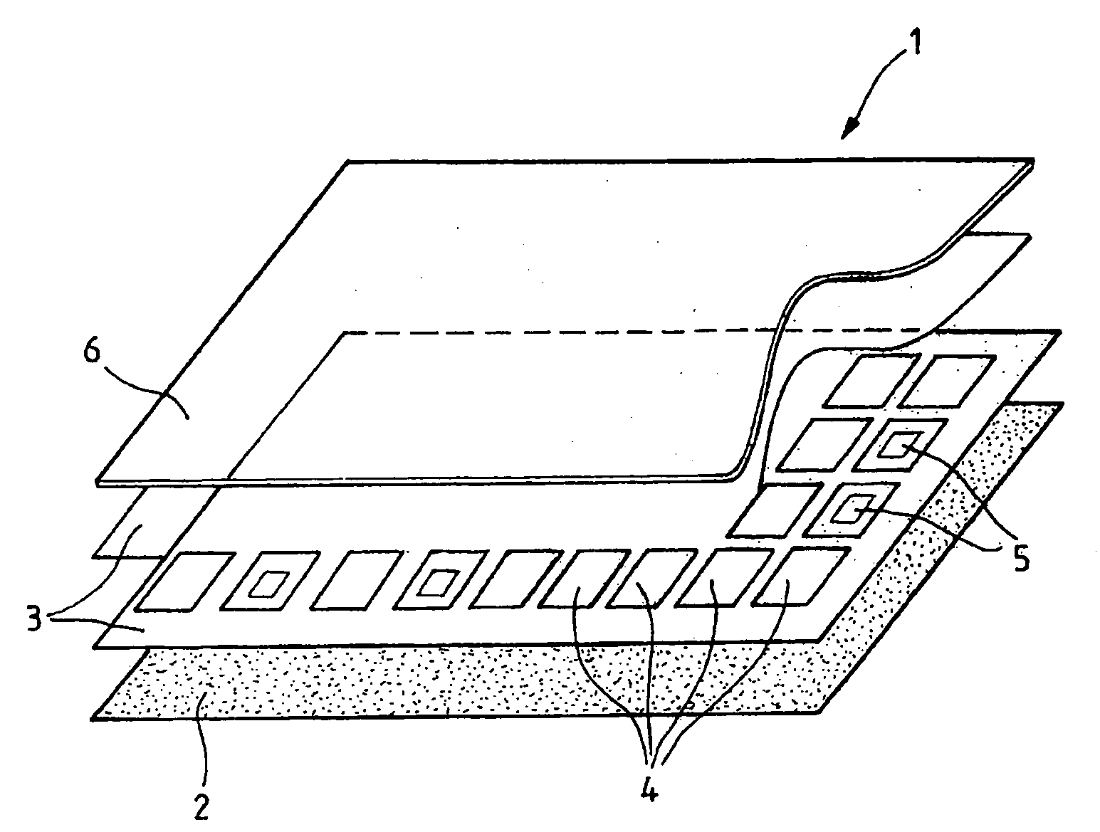
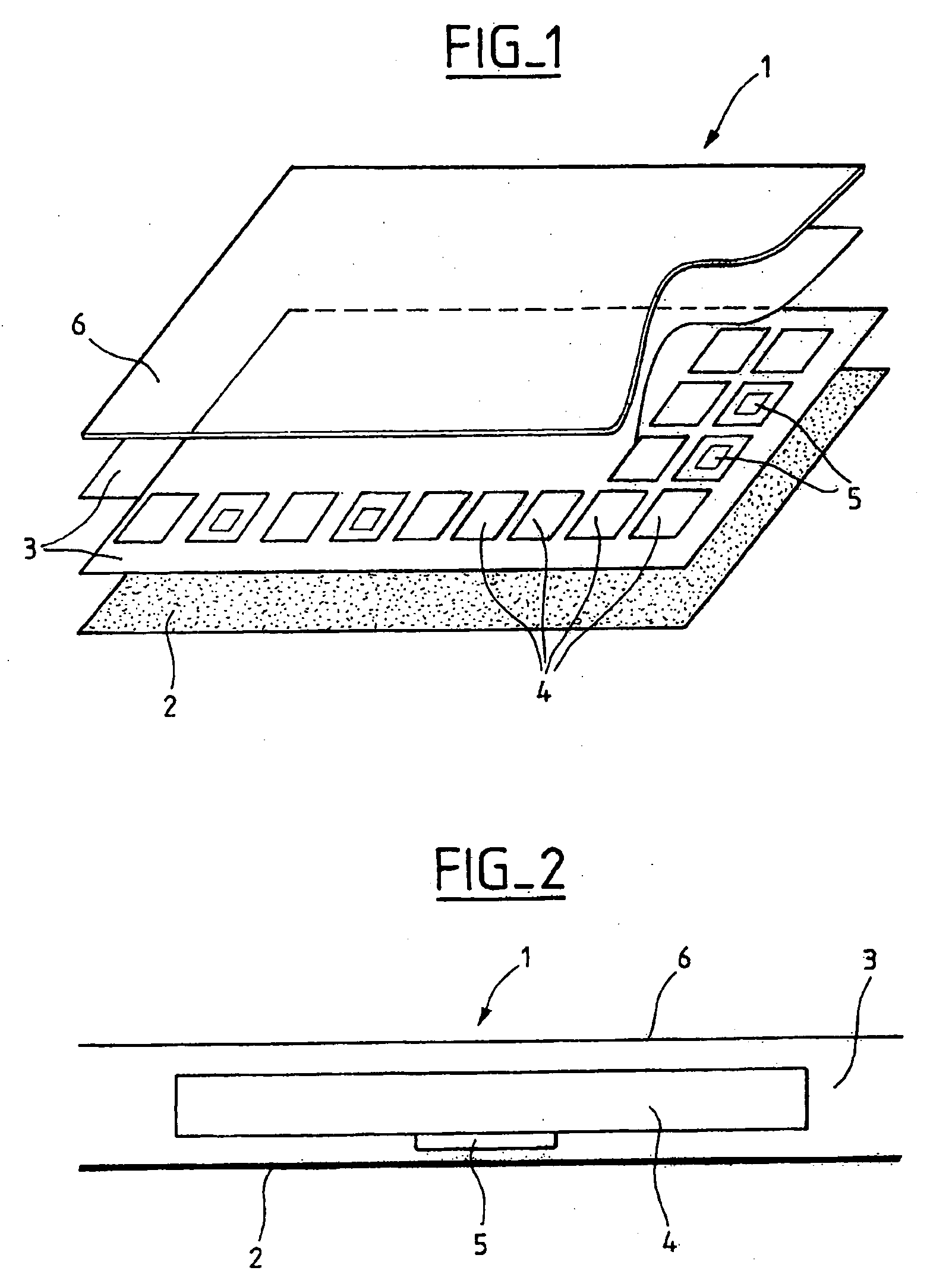
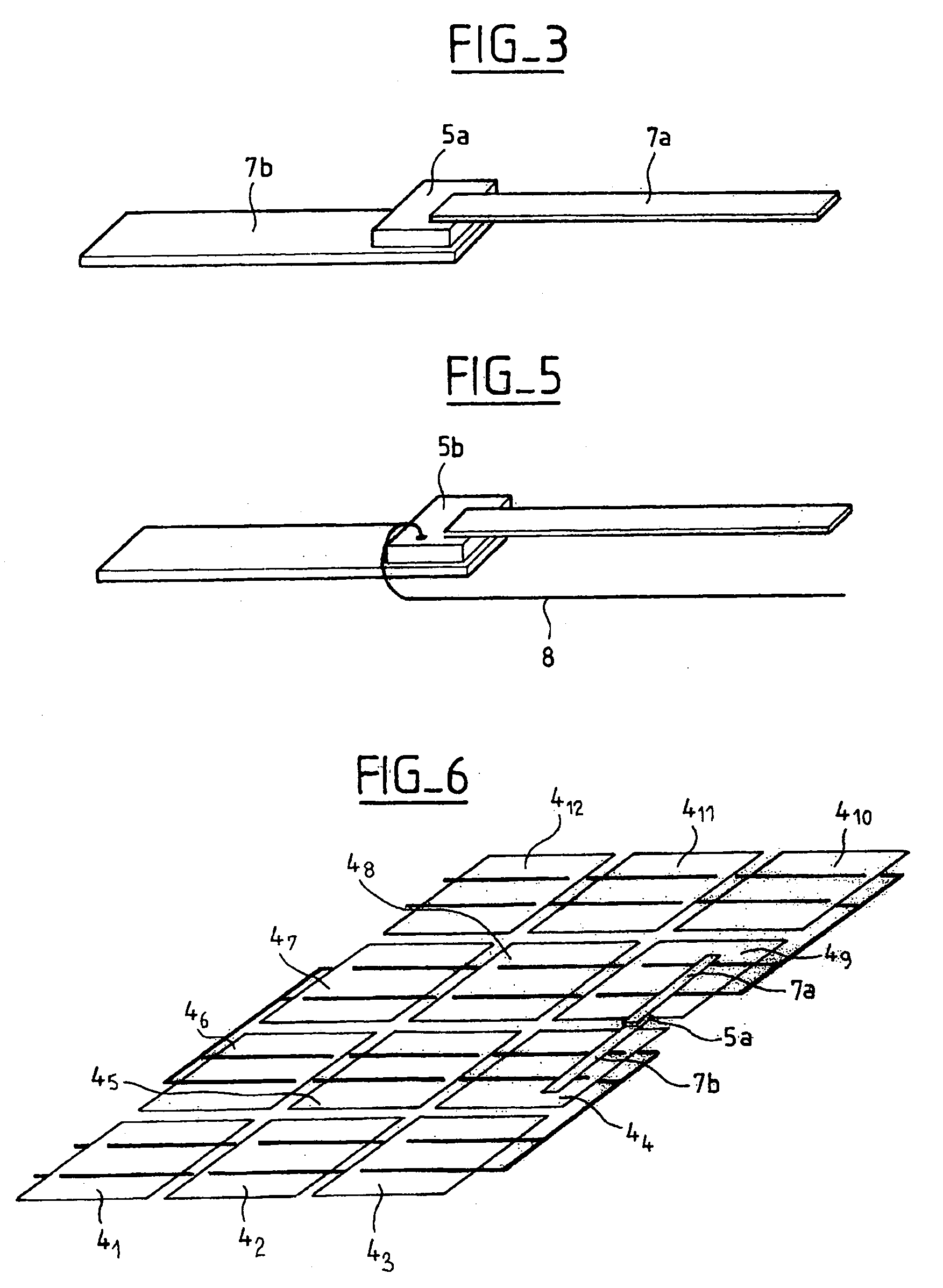
[0041]FIG. 1 is a diagram showing a laminated stack of a photovoltaic module 1 of the invention presenting a plurality of parallel layers stacked one on another. The back of the photovoltaic module 1 is formed by a layer of strong polymer, e.g. a sheet of Tedlar®, having deposited thereon an encapsulating polymer 3, e.g. EVA. Inside the encapsulated polymer there are arranged photovoltaic cells 4 in a common plane and ordered in a grid with their rear faces facing towards the layer 2, together with semiconductor circuits 5 placed under some of the photovoltaic cells 4. Finally, the encapsulating polymer 3 has a plate of glass 6 placed thereon to form the front of the photovoltaic module.

[0042] For the purpose of securing the photovoltaic cells 4 and the semiconductor circuits 5, the encapsulating polymer 3 can be cured in a vacuum and at a temperature of about 150° C. for EVA. The layer 2 of strong polymer then provides sealing and protection against mechanical damage to the back o...


PUM


Abstract

A photovoltaic module including one or more photovoltaic cells connected in series and located inside a laminated stack of glass and polymer, together with an electronic protection device, e.g. a bypass diode, which is arranged to bypass the electric current passing through at least one photovoltaic cell. The electronic protection device, which is a semiconductor circuit, is itself disposed inside the laminated stack. The semiconductor circuit is electrically connected to at least one flat metal ribbon disposed in the laminated stack for the purpose of dissipating the heat energy given off by the semiconductor circuit.

Description

FIELD OF THE INVENTION [0001] The invention relates to a photovoltaic module which serves in particular for transforming solar energy into electrical energy. BACKGROUND OF THE INVENTION [0002] Such photovoltaic modules are presently designed to deliver electrical power in the range 12 watts (W) to 230 W. They are used in numerous terrestrial applications for providing direct current (DC) or alternating current (AC). For example, they are used in sites that are isolated or that are connected to the power supply distribution network: [0003] in public utility power supply networks; [0004] by individuals: lighting, radio, television (TV), small household appliances; [0005] for public lighting: advertising panels, bus shelters; [0006] for rural electrification; [0007] for pumping; [0008] for telecommunications: infrastructure, relays in the global system for mobile telecommunications (GSM), isolated subscriber equipment; [0009] for signaling: roadside, at sea, radio, TV. [0010] In genera...

Claims


Application Information

Patent Timeline
IPC IPC(8): H01L25/00H01L27/142H01L31/042H01L31/048
CPCH01L31/042H01L31/048Y02E10/50H01L31/046H01L2924/0002H01L2924/00H01L31/0443
Inventor PROISY, BERNARDDUGUE, CHRISTOPHELAPORTE, MICHELLE QUANG, NAM
Owner PHOTOWATT INT
Why Eureka
Try Eureka