
Semiconductor device with a high-k gate dielectric and a metal gate electrode

a high-k gate dielectric and metal gate electrode technology, applied in semiconductor devices, radio frequency controlled devices, electrical apparatuses, etc., can solve the problems of mos field-effect transistors with very thin gate dielectrics made from silicon dioxide that may experience unacceptable gate leakage currents and react adversely with high-k gate dielectrics

Active Publication Date: 2006-01-26
INTEL CORP
View PDF27 Cites 45 Cited by
  • Summary
  • Abstract
  • Description
  • Claims
  • Application Information

AI Technical Summary

Benefits of technology

The present invention relates to a semiconductor device with a high-k gate dielectric and metal gate electrodes. The invention provides a solution for reducing gate leakage currents and improving the thermal stability of the device. The use of a metal gate electrode with an aluminide composition that has a workfunction below 4.3 eV and is thermally stable at 400° C. ensures compatibility with the high-k gate dielectric and prevents unwanted reactions with the dielectric. The invention also provides a method for making the semiconductor device with the desired features.

Problems solved by technology

MOS field-effect transistors with very thin gate dielectrics made from silicon dioxide may experience unacceptable gate leakage currents.
Because, however, such a dielectric may not be compatible with polysilicon, it may be desirable to use metal gate electrodes in devices that include high-k gate dielectrics.
Those metals, however, may be thermally unstable at temperatures above 400° C., causing them to react adversely with high-k gate dielectrics.

Method used


Image

  • Semiconductor device with a high-k gate dielectric and a metal gate electrode
  • Semiconductor device with a high-k gate dielectric and a metal gate electrode
  • Semiconductor device with a high-k gate dielectric and a metal gate electrode

Examples


Embodiment Construction

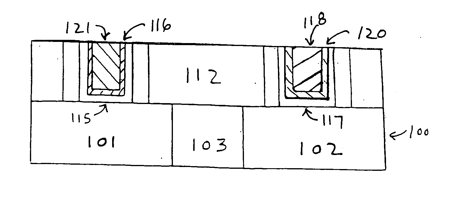
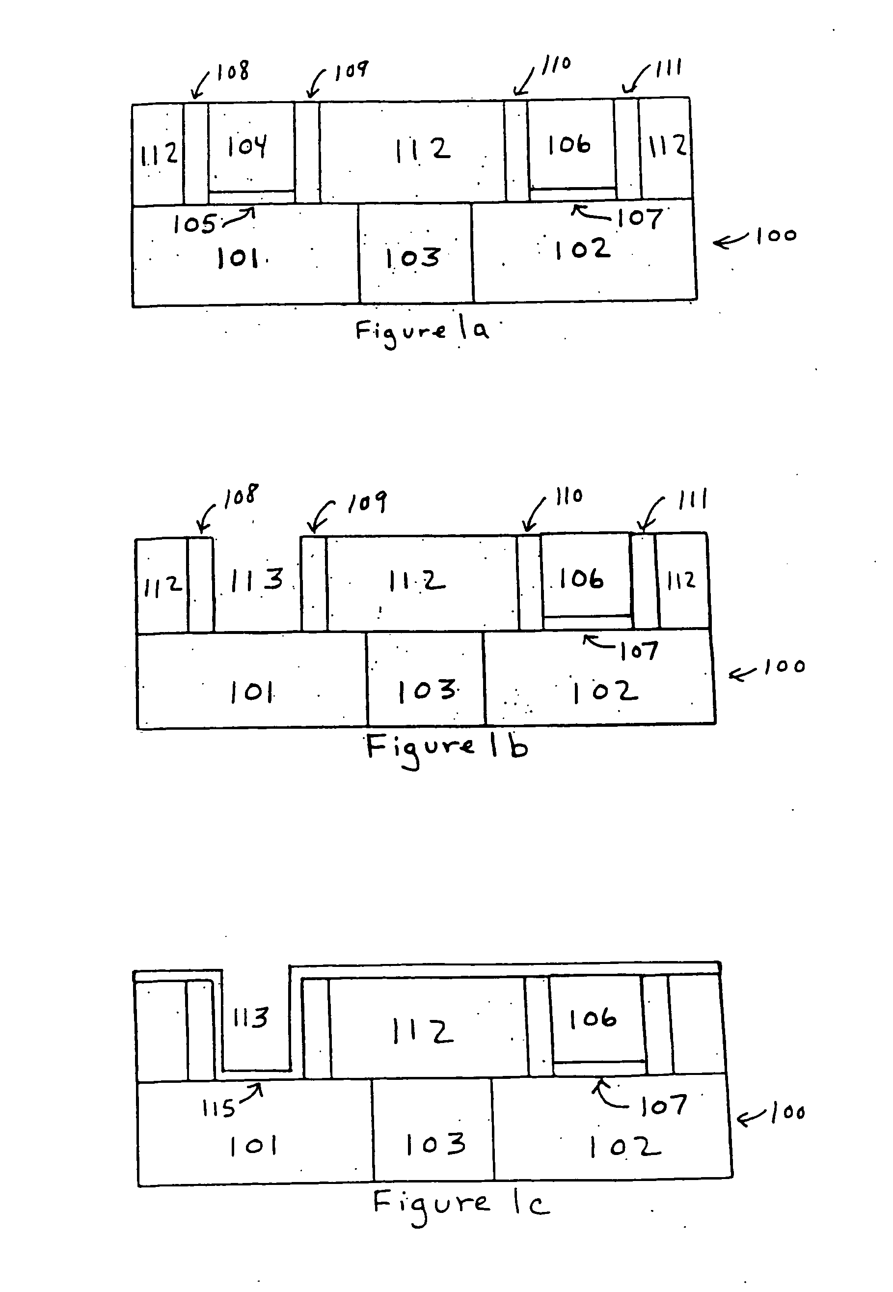
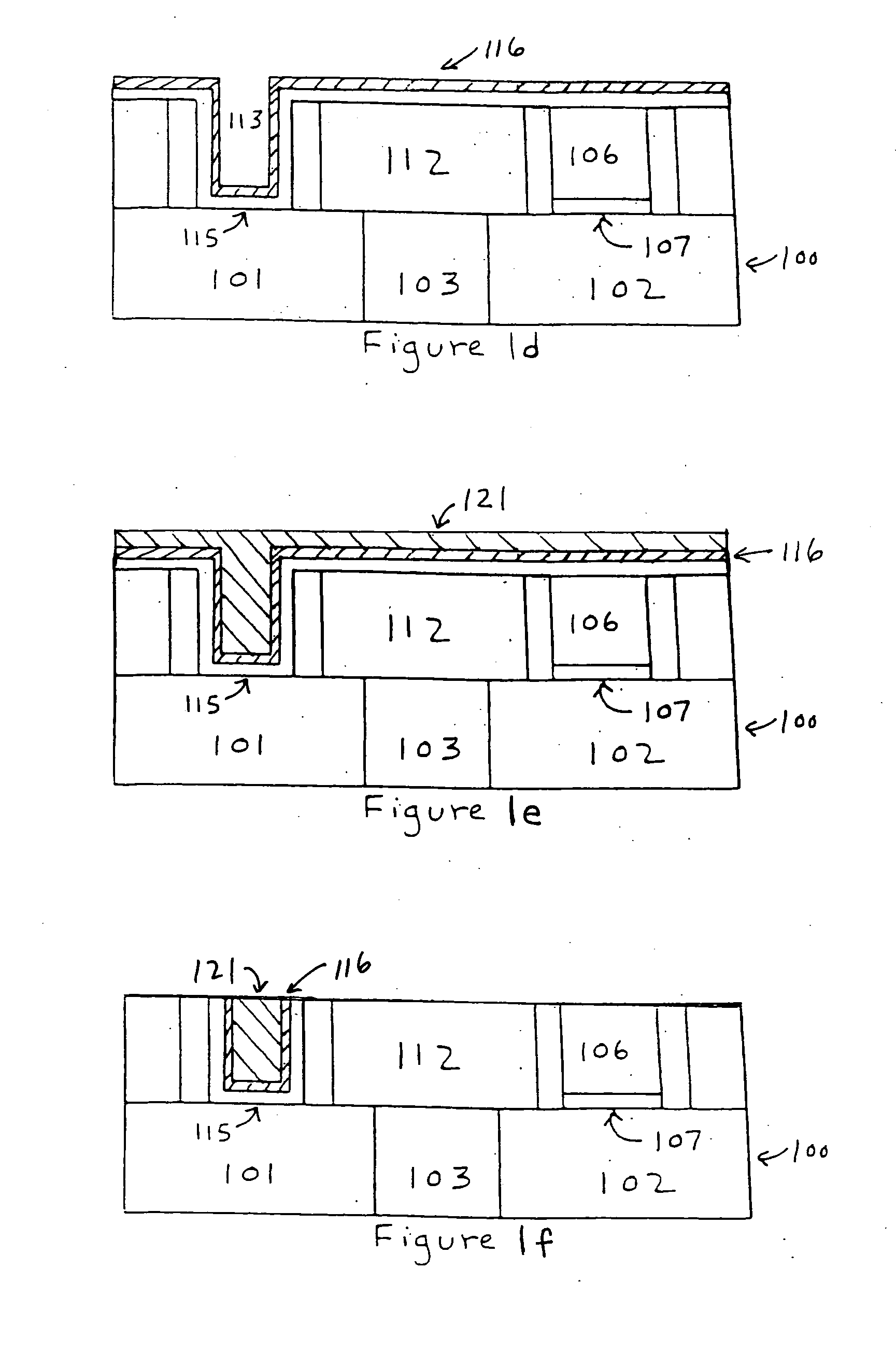
[0006] A semiconductor device is described. That semiconductor device comprises a gate dielectric and a metal gate electrode that comprises an aluminide. In the following description, a number of details are set forth to provide a thorough understanding of the present invention. It will be apparent to those skilled in the art, however, that the invention may be practiced in many ways other than those expressly described here. The invention is thus not limited by the specific details disclosed below.

[0007] One embodiment of the present invention comprises a high-k gate dielectric upon which is formed an NMOS metal gate electrode that comprises an aluminide. The high-k gate dielectric may comprise hafnium oxide, hafnium silicon oxide, lanthanum oxide, lanthanum aluminum oxide, zirconium oxide, zirconium silicon oxide, titanium oxide, tantalum oxide, barium strontium titanium oxide, barium titanium oxide, strontium titanium oxide, yttrium oxide, aluminum oxide, lead scandium tantalum ...


PUM


Abstract

A semiconductor device is described that comprises a gate dielectric and a metal gate electrode that comprises an aluminide.

Description

FIELD OF THE INVENTION [0001] The present invention relates to semiconductor devices, in particular, those that include high-k gate dielectrics and metal gate electrodes. BACKGROUND OF THE INVENTION [0002] MOS field-effect transistors with very thin gate dielectrics made from silicon dioxide may experience unacceptable gate leakage currents. Forming the gate dielectric from certain high-k dielectric materials, instead of silicon dioxide, can reduce gate leakage. Because, however, such a dielectric may not be compatible with polysilicon, it may be desirable to use metal gate electrodes in devices that include high-k gate dielectrics. Certain metals with a workfunction below 4.3 eV may be used to make metal gate electrodes for NMOS transistors. Those metals, however, may be thermally unstable at temperatures above 400° C., causing them to react adversely with high-k gate dielectrics. [0003] Accordingly, there is a need for a semiconductor device with a high-k gate dielectric, and an N...

Claims


Application Information

Patent Timeline
Patent Type & Authority Applications(United States)
IPC IPC(8): H01L29/76
CPCH01L21/28194H01L21/823842H01L29/66545H01L29/517H01L29/518H01L29/4966H01L21/18H01L21/8238
Inventor DOCZY, MARK L.KAVALIEROS, JACKMETZ, MATTHEW V.BRASK, JUSTIN K.DATTA, SUMANCHAU, ROBERT S.
Owner INTEL CORP
Learn More