Method of refining scrap silicon using an electron beam

a technology of scrap silicon and electron beam, which is applied in the direction of silicon compounds, electric furnaces, furnaces, etc., can solve the problems of inability to refine scraps, inability to obtain high-purity silicon, and inability to achieve high-purity silicon, etc., and achieves short period of time and good efficiency

Inactive Publication Date: 2006-01-26
IIS MATERIALS CORP
View PDF2 Cites 4 Cited by
  • Summary
  • Abstract
  • Description
  • Claims
  • Application Information

AI Technical Summary

Benefits of technology

[0013] In a refining method for scrap silicon using an electron beam according to the present invention, lumps of n-type scrap silicon containing a specific impurity element as a dopant are selectively prepared, the prepared lumps of scrap silicon are crushed, the crushed silicon is irradiated with an electron beam in a vacuum vessel and melted and at least a portion of the impurity element is vaporized, and the resulting molten silicon is solidified. Therefore, high-purity silicon can be manufactured from scrap silicon in a short period of time and with good efficiency. In addition, if a step of supplying a portion of the granular silicon in a holding portion of a vacuum vessel to a hearth provided in the vacuum vessel and irradiating the granular silicon in the hearth with an electron beam to melt it and obtaining molten silicon from which at least a portion of an impurity element was vaporized, a step of transferring the molten silicon to a crucible provided in the vacuum vessel, and a step of irradiating the molten silicon which was transferred to the crucible with an electron beam to further vaporize the specific impurity element are repeated a prescribed number of times, refining operation can be continuously carried out and refining of silicon can be efficiently performed.

Problems solved by technology

However, scrap silicon contains impurities, so it is necessary to increase its purity before it can be reused.
Depending upon the type of impurity element, some lumps cannot be refined using an electron beam, while there are lumps for which refining with an electron beam is possible but is nevertheless impractical from the standpoints of refining time and refining costs.
In addition, when lumps of scrap silicon containing different impurity elements are mixed together during the melting stage of a refining process, high-purity silicon is not obtained.
Furthermore, if scrap silicon contains impurity elements which cannot be removed adequately or at all by melting, the impurity elements end up remaining in the silicon after refining, and high-purity silicon is not obtained.

Method used


Image

  • Method of refining scrap silicon using an electron beam
  • Method of refining scrap silicon using an electron beam
  • Method of refining scrap silicon using an electron beam

Examples


Embodiment Construction

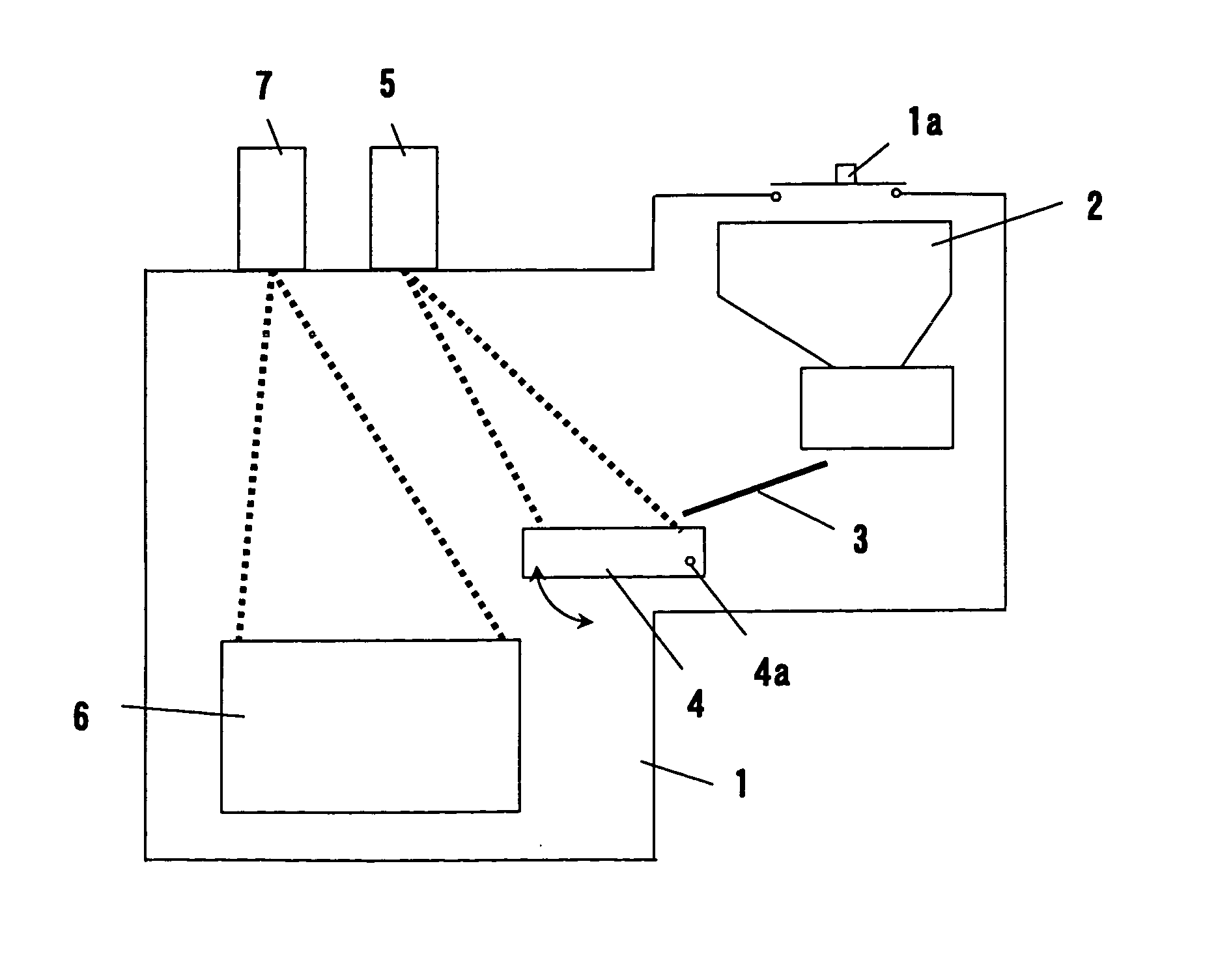
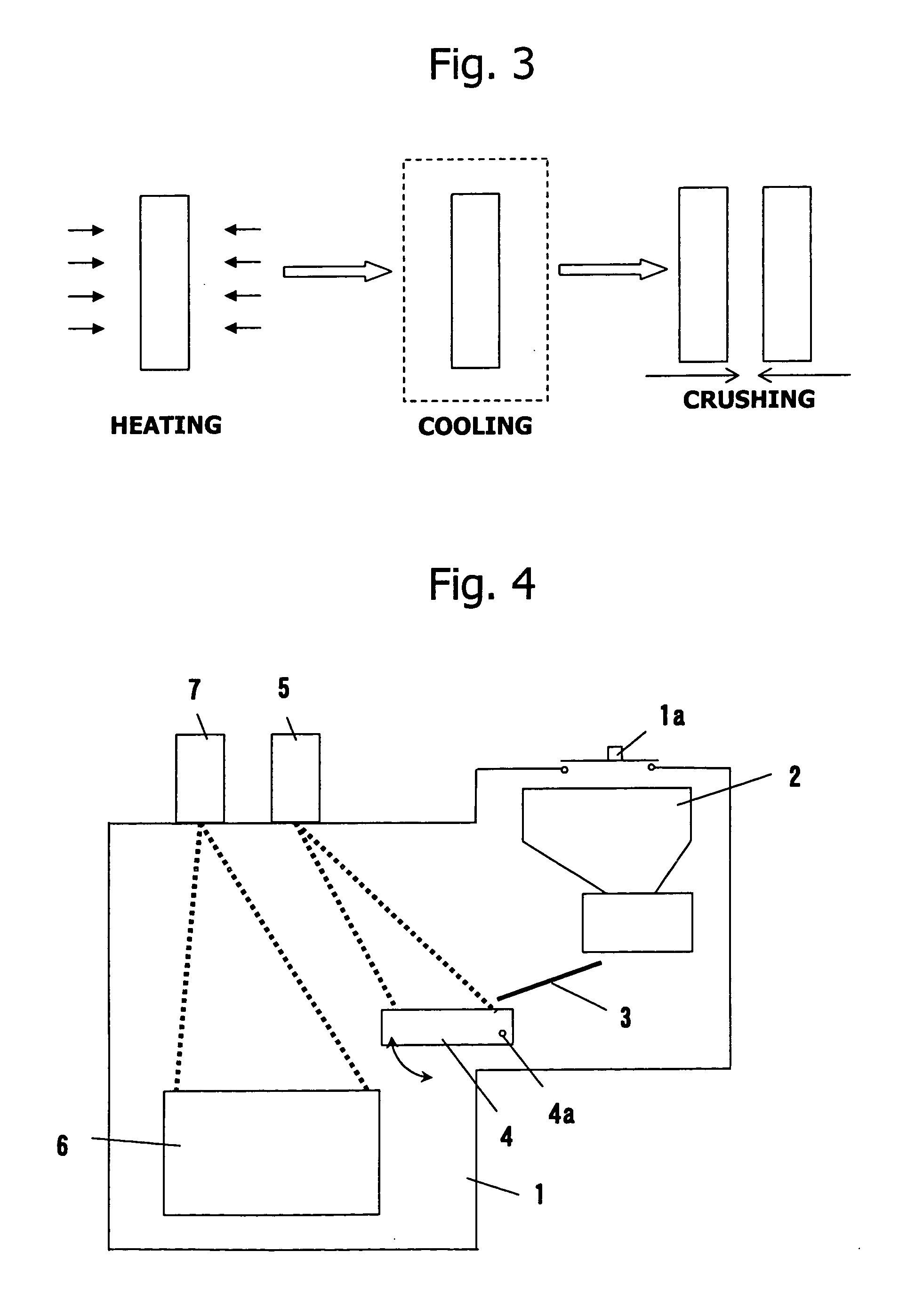
[0021] Below, an embodiment of a refining method for scrap silicon using an electron beam according to the present invention will be described while referring to the accompanying drawings.

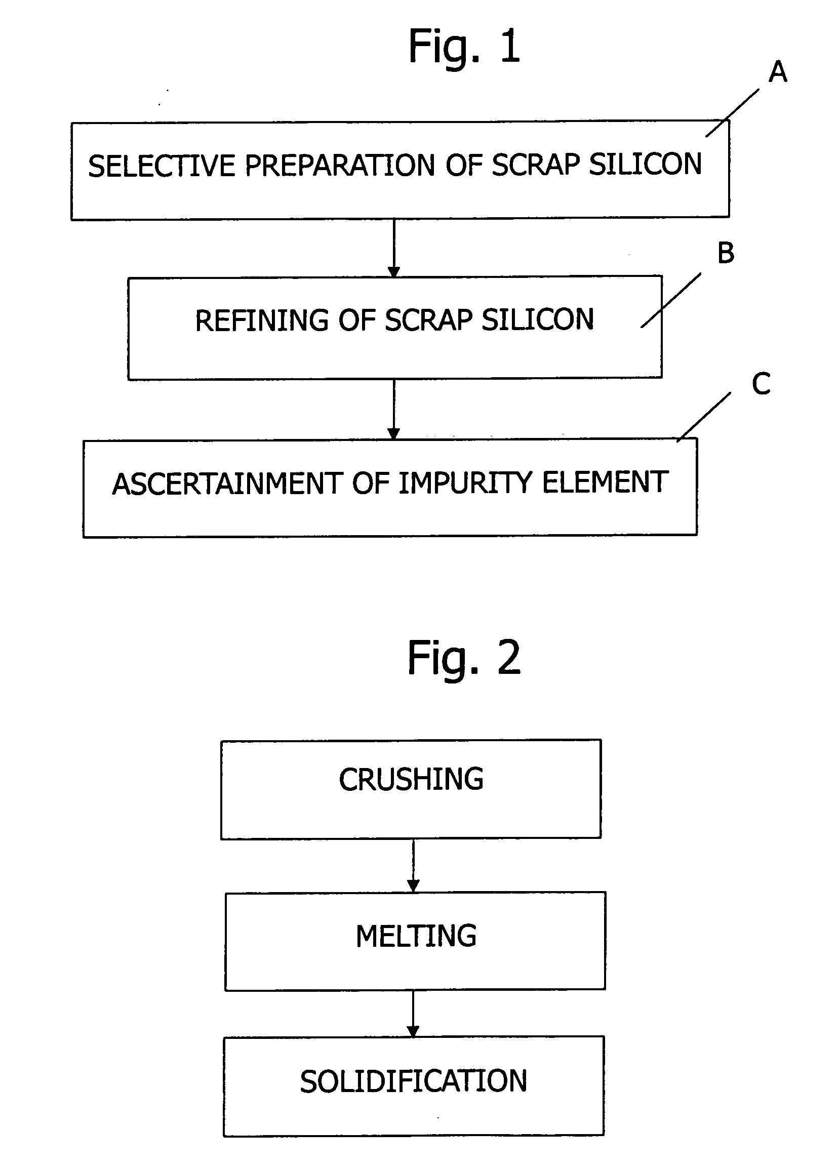
[0022] As shown in FIG. 1, this embodiment of a method of refining scrap silicon using an electron beam according to the present invention includes Step A of selectively preparing lumps of n-type scrap silicon containing a specific impurity element as a dopant, Step B of refining the scrap silicon to manufacture product silicon, and Step C of analyzing the manufactured product silicon and again ascertaining whether the prepared lumps of scrap silicon contained the specific impurity element as a dopant. These steps will be described in detail below.

Step A (Preparation Step)

[0023] First, lumps of n-type scrap silicon containing a specific impurity element as a dopant, such as lumps of n-type scrap silicon containing antimony as a dopant, are selectively prepared. Namely, lumps of n-type scrap sil...


PUM

PropertyMeasurementUnit
pressureaaaaaaaaaa
temperatureaaaaaaaaaa
angleaaaaaaaaaa

Abstract

A method of refining scrap silicon using an electron beam includes a step of selectively preparing lumps of n-type scrap silicon containing a specific impurity element as a dopant, a step of crushing the prepared lumps of scrap silicon, a step of placing the crushed silicon into a vacuum vessel, a step of irradiating the crushed silicon which was placed into the vacuum vessel with an electron beam to melt it and vaporize at least a portion of the impurity element, and a step of solidifying the resulting silicon.

Description

BACKGROUND OF THE INVENTION [0001] This invention relates to a method which can refine scrap silicon rapidly and in large quantities using an electron beam to obtain high-purity silicon suitable for solar cells, semiconductors, and similar devices. [0002] In order to increase the rate of utilization of silicon raw materials, it is desired to reutilize scrap which is produced during the manufacture of silicon wafers from silicon ingots (referred to below as “scrap silicon”). However, scrap silicon contains impurities, so it is necessary to increase its purity before it can be reused. [0003] Japanese Published Unexamined Patent Application Hei 10-245216 discloses that the yield of silicon can be increased by recovering scrap silicon which is produced during the manufacture of silicon for solar cells and returning the recovered scrap silicon to a refining step. [0004] However, that document merely discloses a technique for improving the yield of silicon in the manufacture of silicon fo...

Claims


Application Information

Patent Timeline
Patent Type & Authority Applications(United States)
IPC IPC(8): C22B9/22C01B33/037
CPCC01B33/037
Inventor YAMAUCHI, NORICHIKASHIMADA, TAKEHIKO
Owner IIS MATERIALS CORP
Why Eureka
Try Eureka