Method for fabricating metal line in a semiconductor

a metal line and semiconductor technology, applied in semiconductor/solid-state device manufacturing, basic electric elements, electric devices, etc., can solve the problems of increasing the time for the planarization process and the cost of the process, and achieve the effects of enhancing the planarity of metal lines, reducing the removal rate of metal layers, and improving the performance and yield of semiconductor devices

Active Publication Date: 2006-01-12
MARVELL ASIA PTE LTD +1
View PDF7 Cites 5 Cited by
  • Summary
  • Abstract
  • Description
  • Claims
  • Application Information

AI Technical Summary

Benefits of technology

[0015] The present invention has been made in an effort to provide a method for fabricating a metal line in a semiconductor device having advantages of enhancement of performa...

Problems solved by technology

However, forming such a dummy pattern may increase ...

Method used


Image

  • Method for fabricating metal line in a semiconductor
  • Method for fabricating metal line in a semiconductor
  • Method for fabricating metal line in a semiconductor

Examples


Embodiment Construction

[0021] An embodiment of the present invention will hereinafter be described in detail with reference to the accompanying drawings.

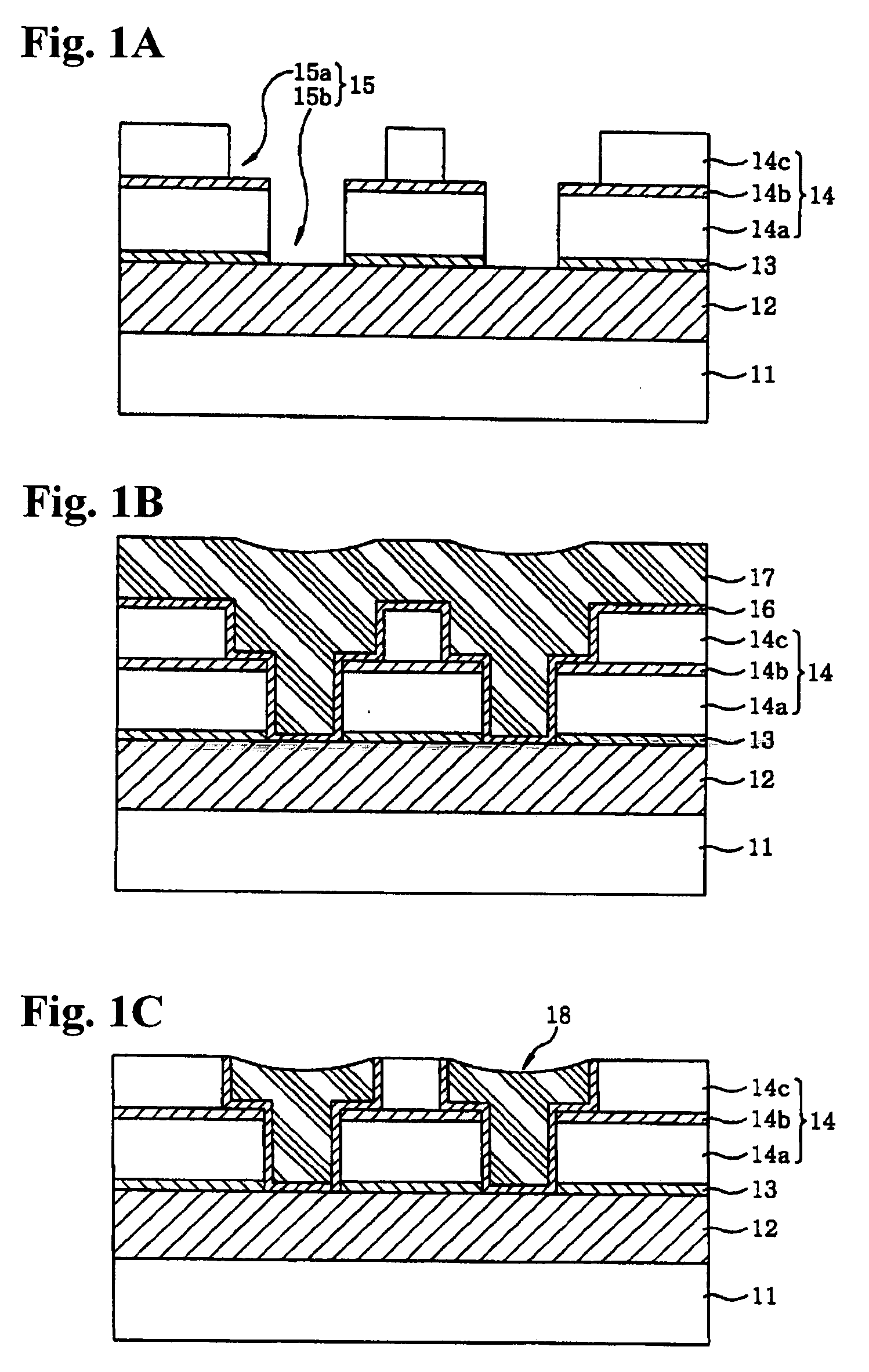
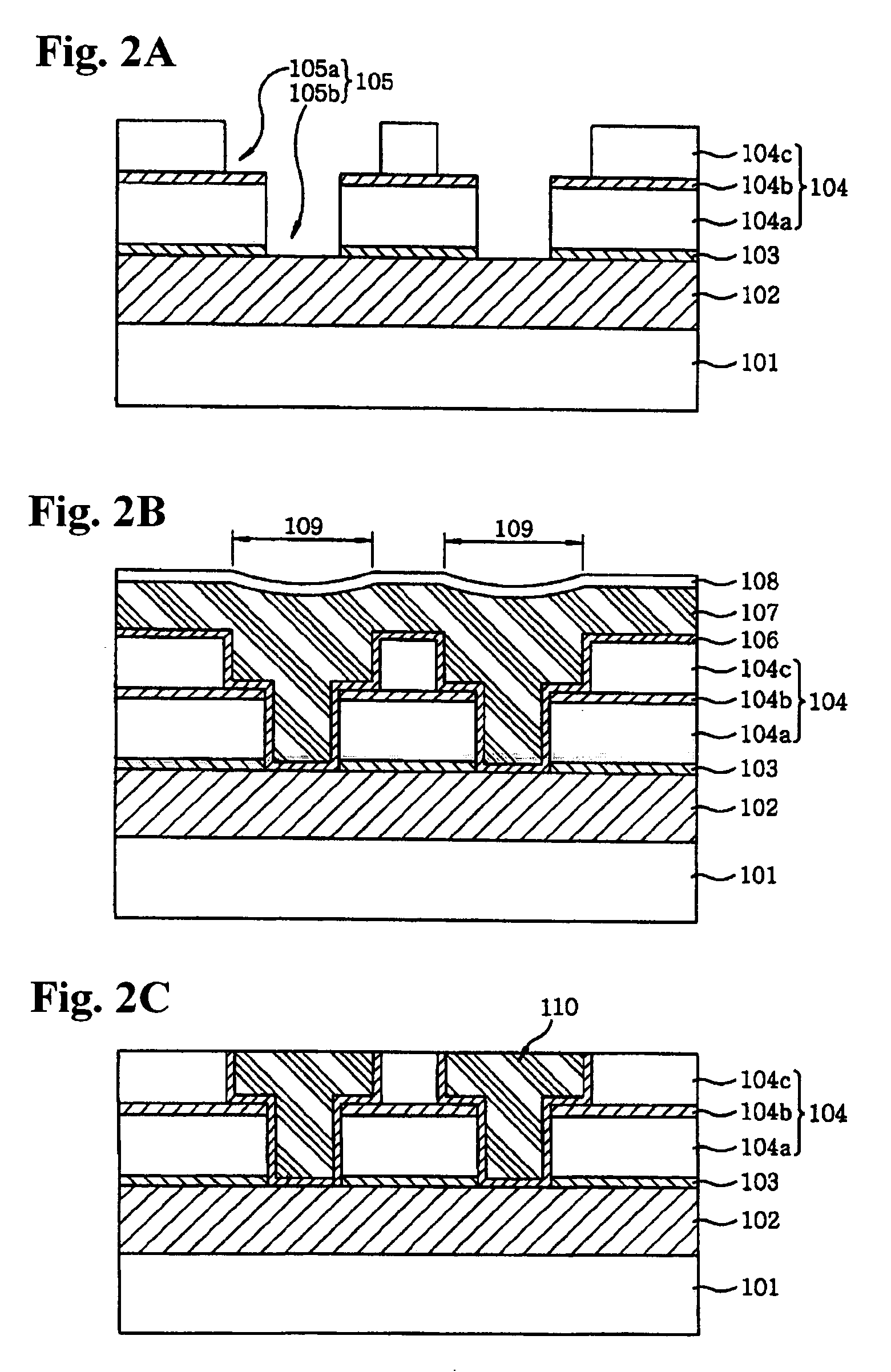
[0022]FIG. 2A to FIG. 2C are sectional views illustrating a process of forming a multiple layer metal line in a semiconductor device according to an exemplary embodiment of the present invention.

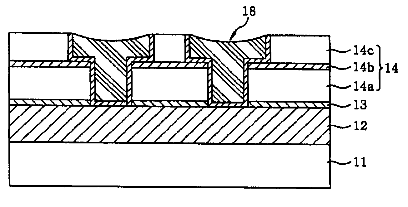
[0023] As shown in FIG. 2A, a lower metal line 102 is formed on a semiconductor substrate 101 having various circuit element structures for a semiconductor thereon and / or therein, generally by conventional photolithographic processing. Thus, the lower metal line 102 generally comprises aluminum or a conventional Al—Cu alloy, which may have one or more barrier layers thereunder (e.g., a stacked Ti / TiN bilayer) and / or one or more capping layers thereover (e.g., a stacked Ti / TiN or Ti / TiW bilayer). Then, a first etch stop layer 103 (e.g., comprising silicon nitride) is formed on the substrate 101 having the lower metal line 102. Subsequently, a first insulating lay...


PUM


Abstract

A metal line is fabricated in a semiconductor device by a method including: forming an etch stop layer on a substrate; forming an interlayer insulating layer on the etch stop layer, the interlayer insulating layer including dual damascene patterns, each respectively having a trench and a via contact hole; forming a barrier metal layer and a line metal layer on the interlayer insulating layer and in the dual damascene patterns; forming an anti-oxidation layer on above the line metal layer; and forming a metal line in the dual damascene patterns by planarizing an entire surface of the anti-oxidation layer.

Description

CROSS-REFERENCE TO RELATED APPLICATION [0001] This application claims priority to and the benefit of Korean Patent Application 10-2004-0053021, filed in the Korean Intellectual Property Office on Jul. 8, 2004, the entire contents of which are incorporated herein by reference. BACKGROUND OF THE INVENTION [0002] (a) Field of the Invention [0003] The present invention relates to a method for manufacturing a semiconductor device. More particularly, the present invention relates to a method for fabricating a metal line in a semiconductor device. [0004] (b) Description of the Related Art [0005] As a semiconductor device becomes more integrated and smaller sized, a gap between lower and upper metal lines is becoming narrower. When the gap between the lower and upper metal lines becomes narrower, a delay of a time constant may increase and thereby an operation speed of the device may decrease. Therefore, for a narrower gap between the lower and upper metal lines, a semiconductor device shou...

Claims


Application Information

Patent Timeline
IPC IPC(8): H01L21/44
CPCH01L21/7684H01L21/28H01L21/283H01L21/304
Inventor HONG, JI-HO
Owner MARVELL ASIA PTE LTD
Why Eureka
Try Eureka